KiCad 7.x Tutorial – Design PCB
Contents
Create a New Project & Schematic
Please follow the link below to create a new project and circuit diagram ✏️ KiCad 7.x Tutorial – Design Circuit.
Footprint Assignment
1. Open the HelloWrold.kicad_pro project and click HelloWrold.kicad_sch.
2. Select Tools ▶︎ Assign Footprints...
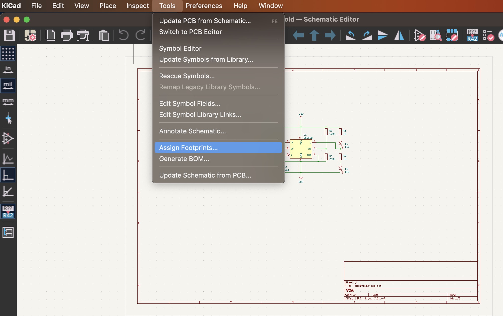
You will see the Assign Footprints window.
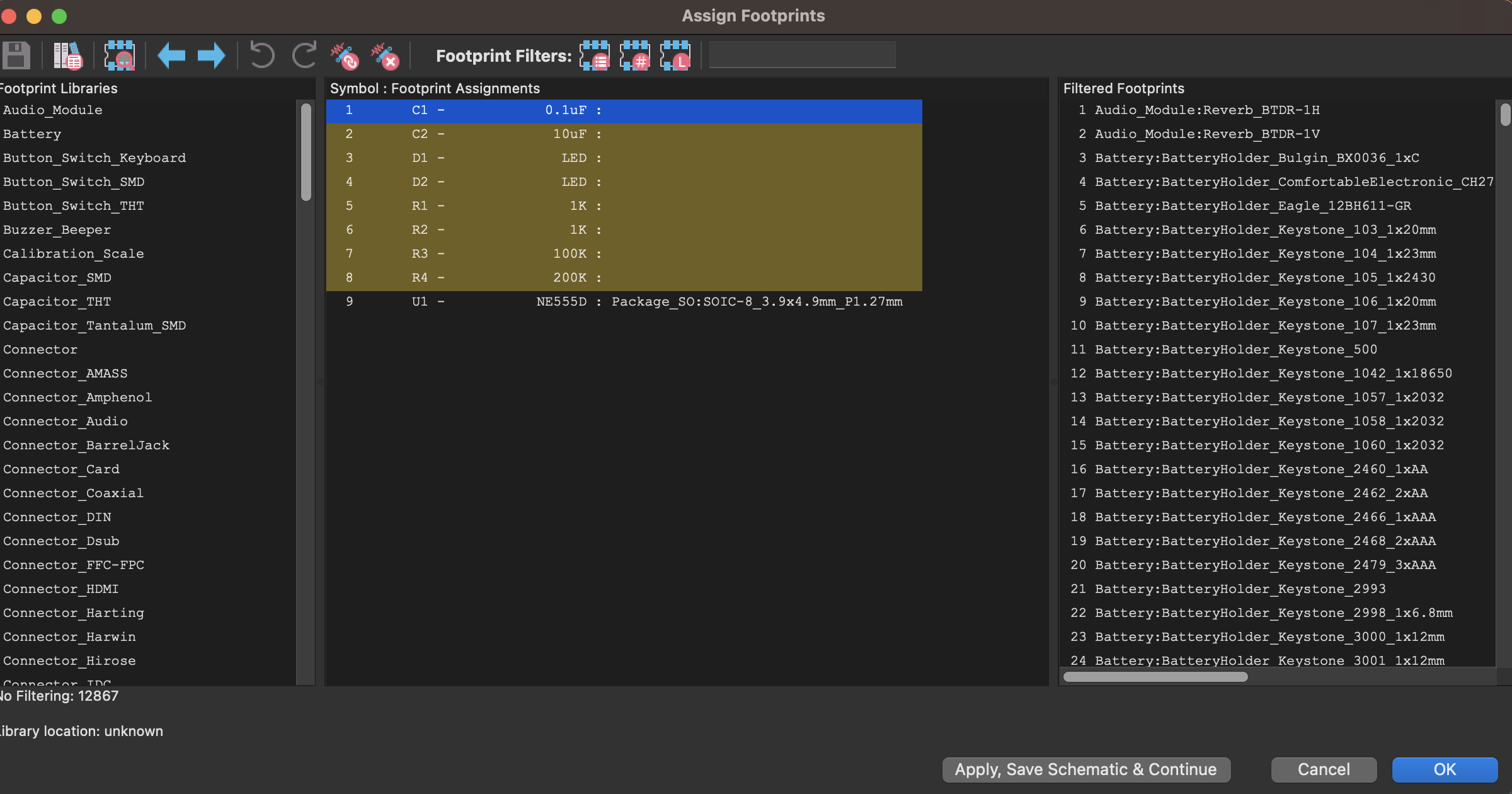
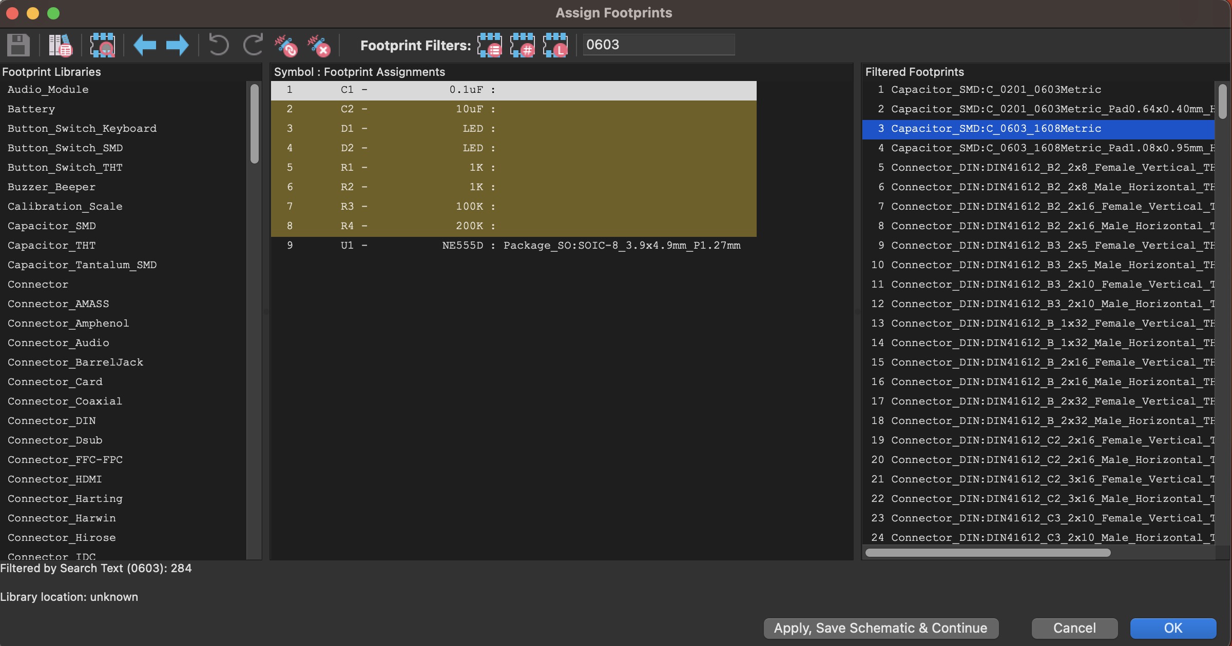
1. Select a component for C1 ▶︎ In Footprint Filters: enter 0603.
2. Select Capacitor_SMD:C_0603_1608Metric in Filtered Footprints.
3. After selecting and clicking it, it will be added to the Symbol : Footprint Assignments.
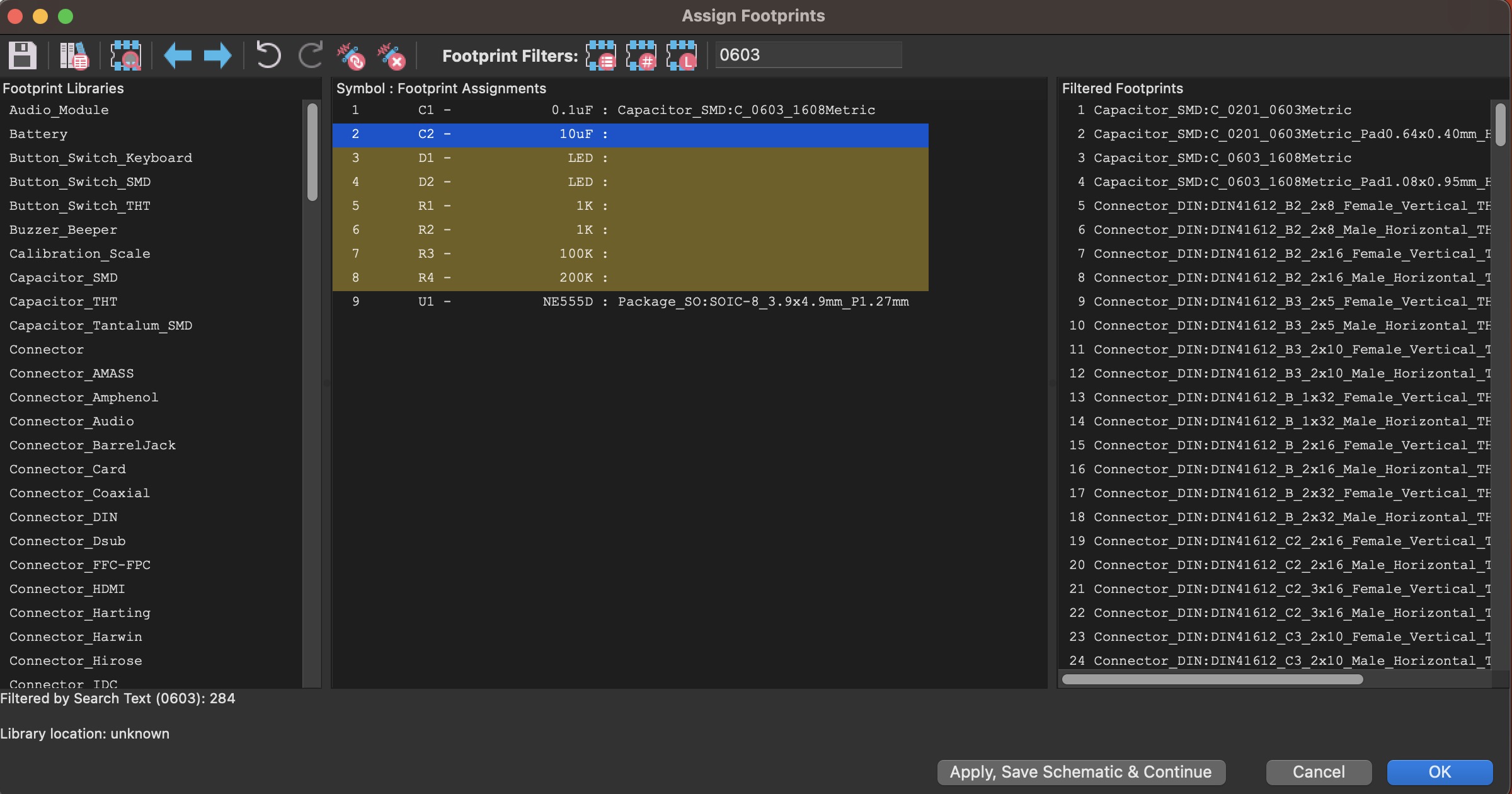
1. Select packaging for C2 ▶︎ In Footprint Filters: enter 0805.
2. Select Capacitor_SMD:C_0603_1608Metric and click to add it.
3. Select packaging for D1 and D2 ▶︎ In Footprint Filters: Enter LED_D.
4. Select LED_THT:LED_D3.0mm and click to add it.
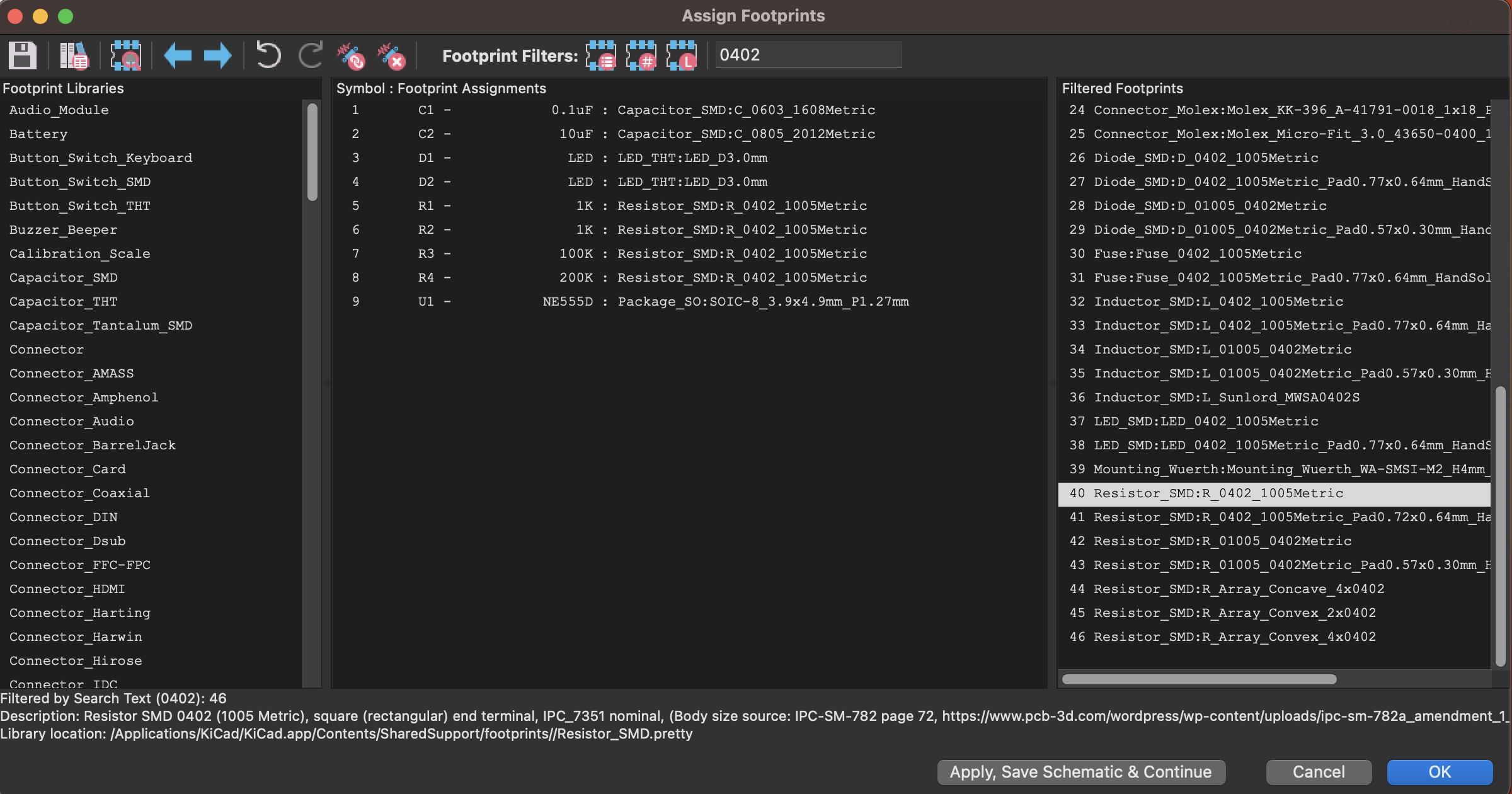
5. Select packaging for R1, R2, R3, R4 ▶︎ In Footprint Filters: enter 0402.
6. Select Resistor_SMD:R_0402_1005Metric and click to add it.
U1 has already been set in the symbol, so there is no need to specify it again. After finishing, click OK as shown below...
Importing Changes From Schematic
Select Tools ▶︎ Update PCB from Schematic... or press F8 ▶︎ Click Update PCB.
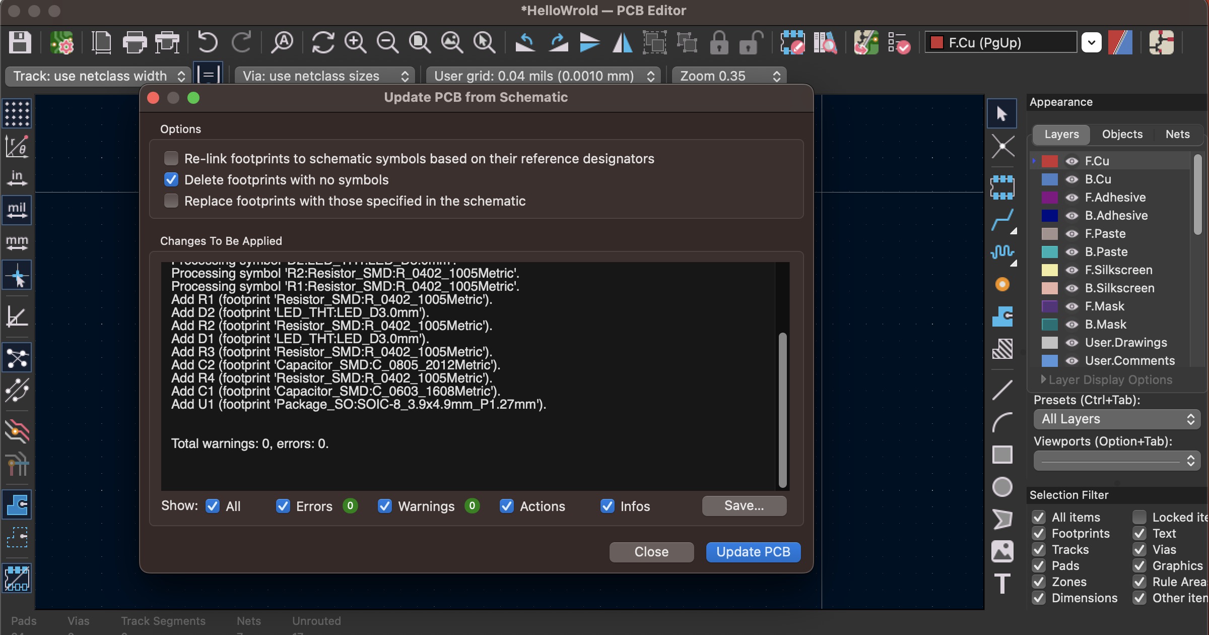
When you click Update PCB, you will see the imported message ▶︎ Click Close.
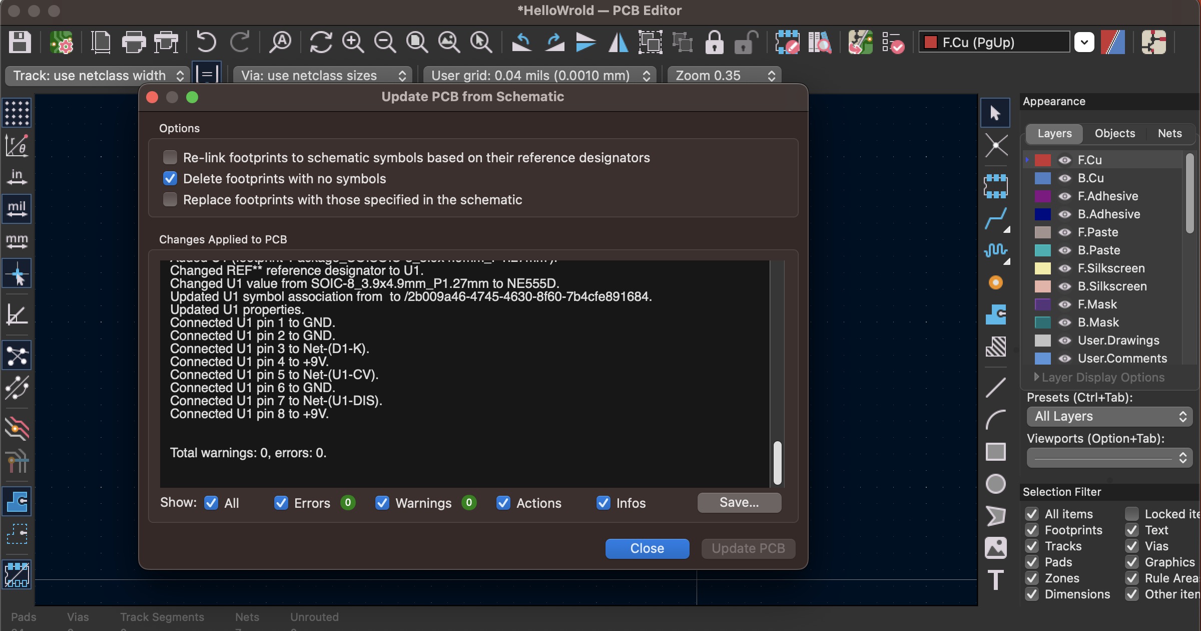
When you click Close, you will see that the imported footprints will be on the mouse, and will be fixed on the drawing after clicking the mouse...
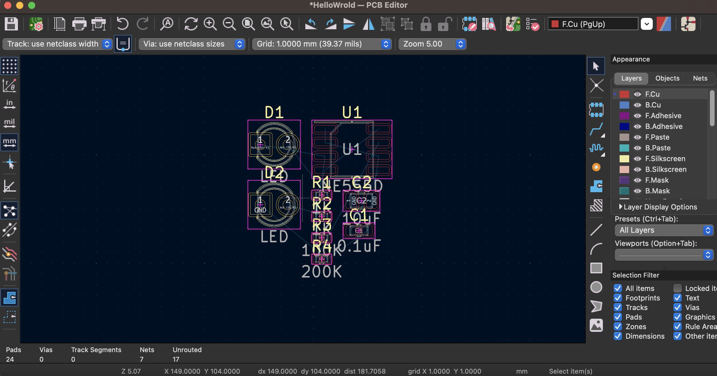
Adding a Board Outline
Click on Edge.Cuts in the layers tab of the Appearance panel on the right (it will be shown with an arrow), as shown below...
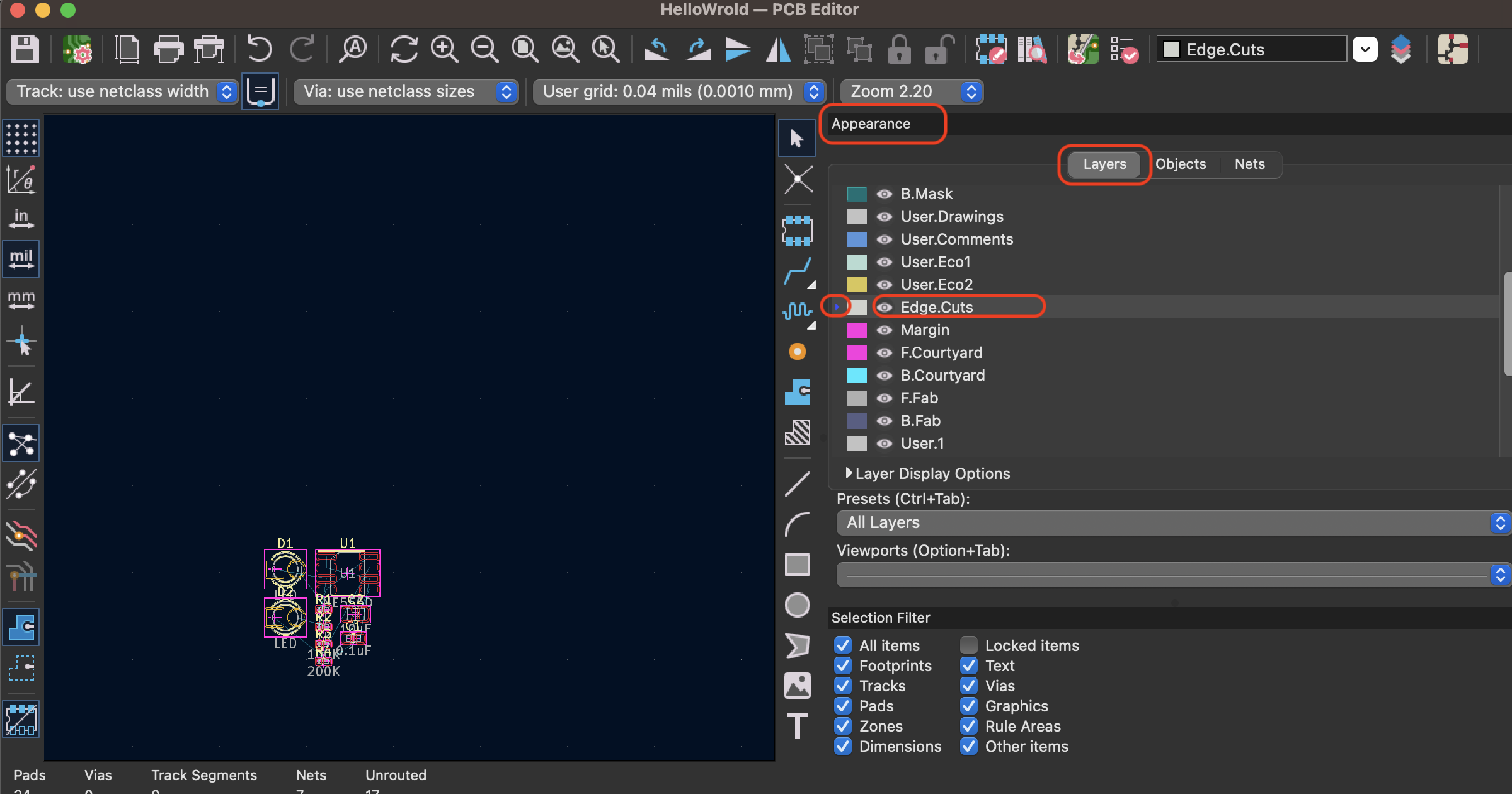
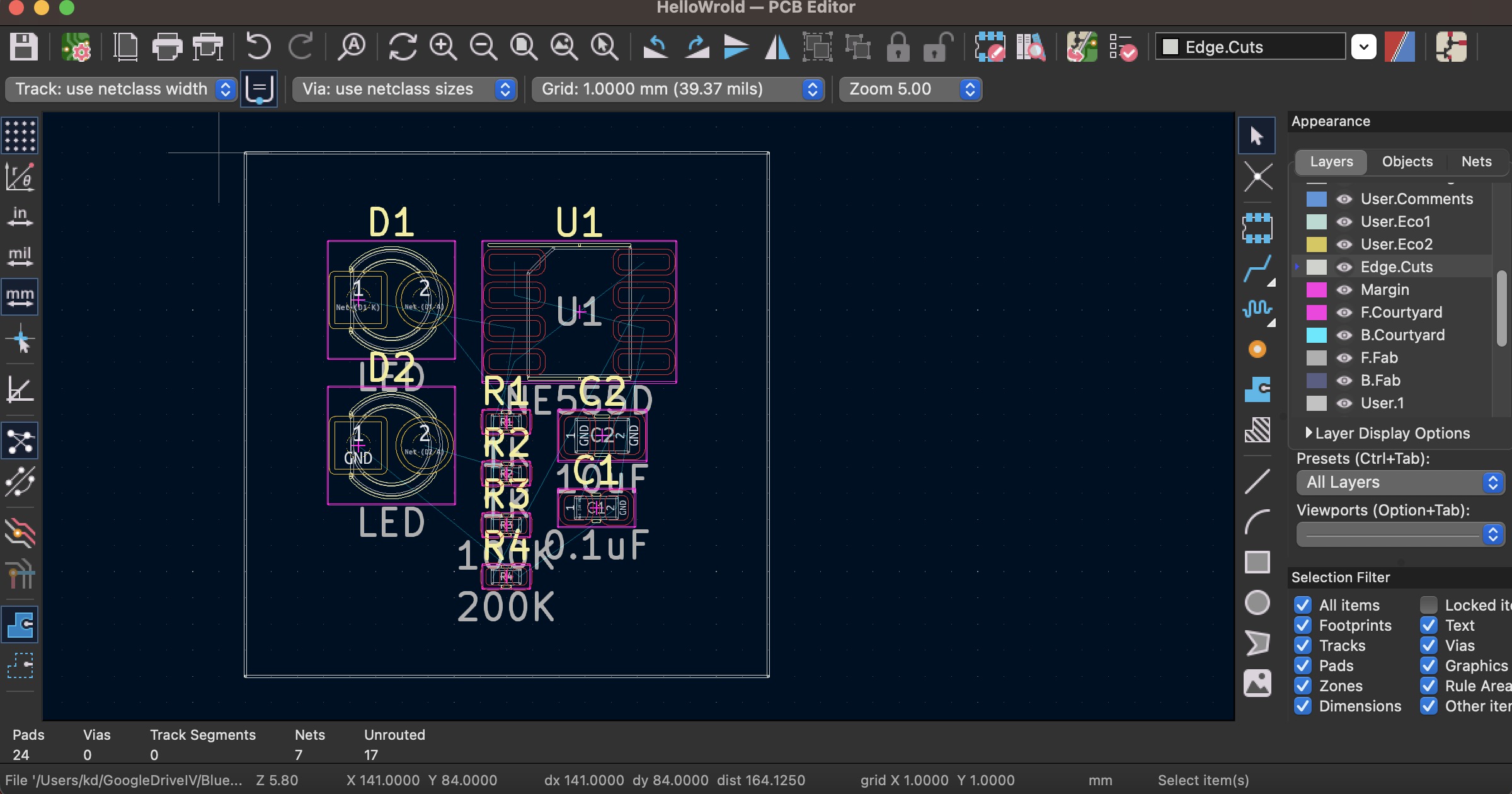
Unit ▶︎ mm ; Grid ▶︎ 1.0000 mm ; Select Place ▶︎ Draw Line.
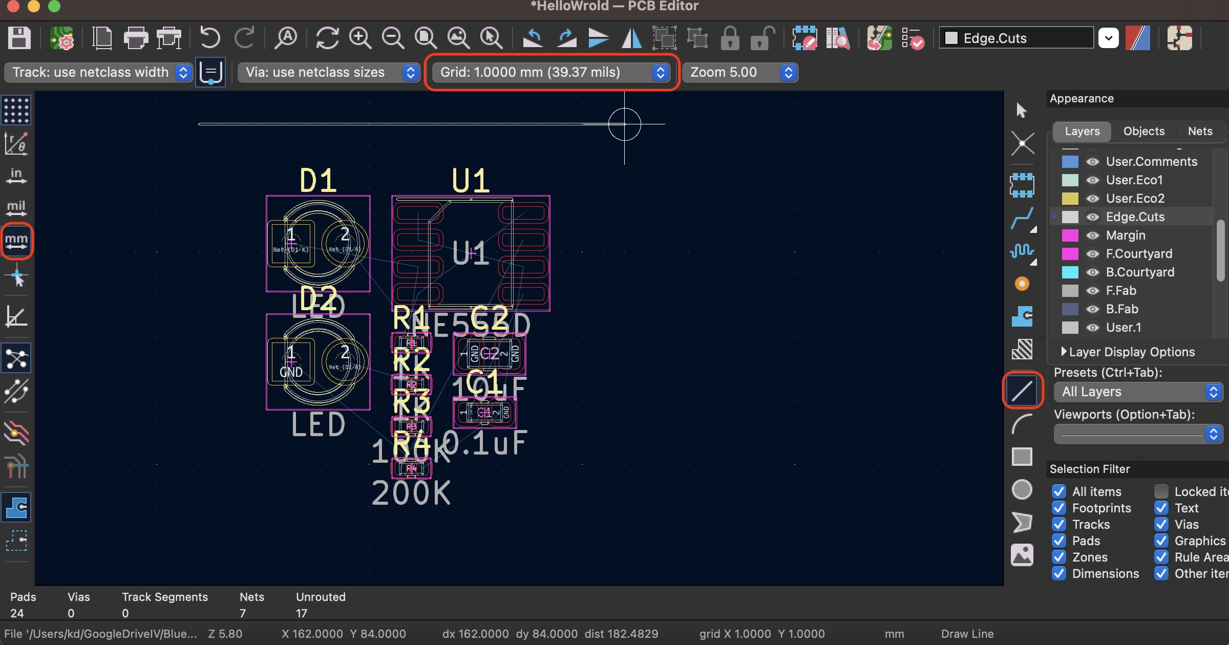
Select the appropriate size to complete the board outline design, as shown below...
Placing Footprints
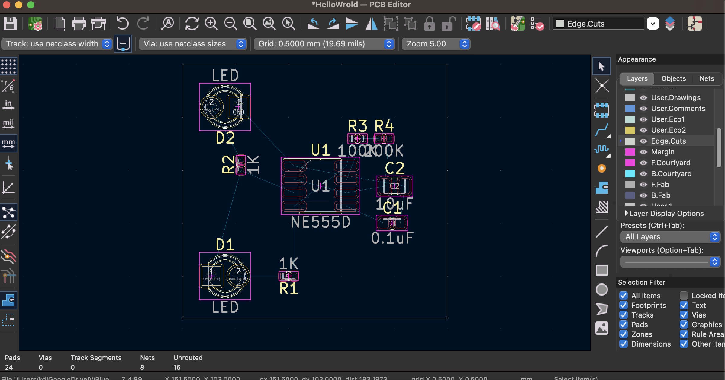
1. Move '+' cursor to the footprint you want to move ▶︎ Press 'm' to move the footprint ▶︎ Press 'r' to rotate the footprint ▶︎ Press 'f' to flip it to the other side.
2. Please arrange all components correctly according to their functions and specifications, as shown below for reference...
Routing
Once the arrangement of the components is completed, the wiring between the 'PAD' of each component can be carried out as follows...
1. Click on F.Cu in the Layers tab of the Appearance panel and set the grid to 0.5000 mm.
2. Select Route ▶︎ Route Single Track or press 'x'.
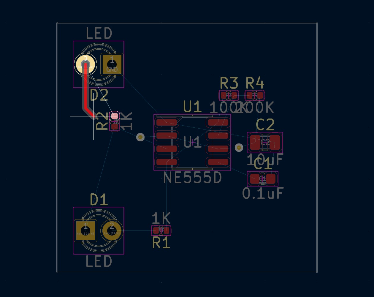
3. Locate the blue unconnected rat wire (ratsnest) between PAD 2 on D2 and PAD 2 on R2.
4. Click the No. 2 PAD of D2 to draw a trace, and then click the No. 2 PAD of R2 to complete the rouitng.
Adding Vias
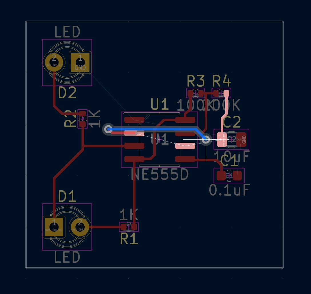
You can add vias to change the routing layer during the routing process, as shown below...
1. Press 'x' and find PAD 2 of U1 and click and pull a trace, press 'v' in the appropriate position to add a via and the trace layer becomes B.Cu.
2. Pull out the appropriate trace on the B.Cu layer and press 'v' again at the appropriate position to add a via and the trace layer becomes F.Cu.
3. Click on PAD 6 of U1 and complete all traces.
Adding Filled Zones
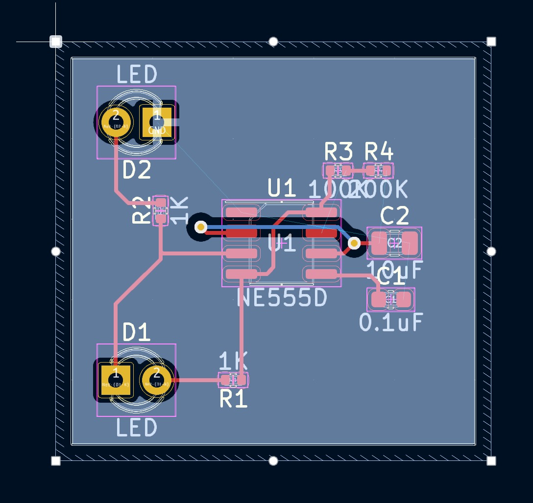
We handle GND with zones as shown below...
1. Click on B.Cu in the Layers tab of the Appearance panel and set the grid to 0.5000 mm.
2. Select Place ▶︎ Add Filled Zone ▶︎ After clicking outside the PCB board frame, a property dialog box will appear.
3. Select 'GND' in Net ▶︎ Click 'OK'.
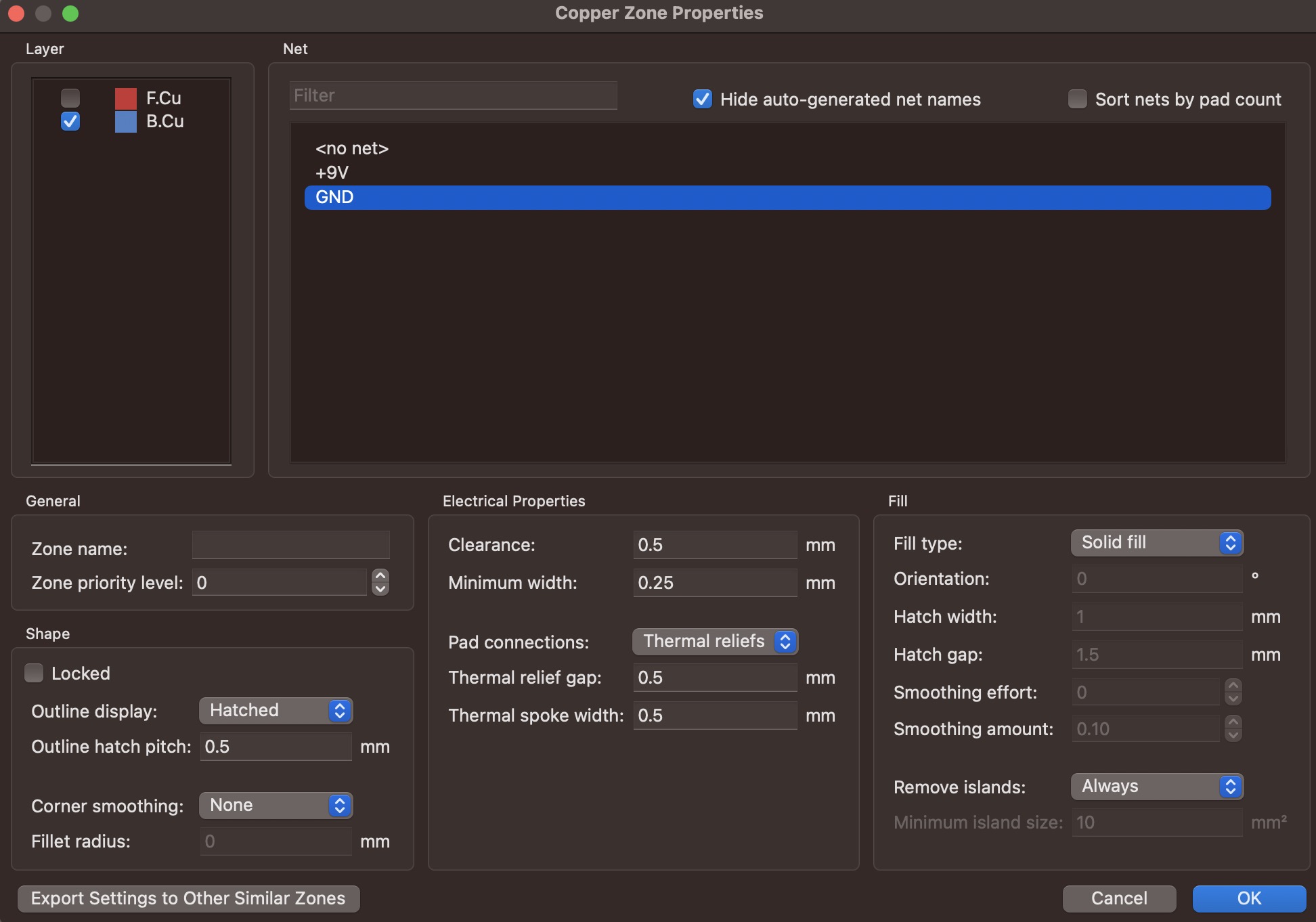
4. Continue to complete the copper laying of GND outside the PCB outline, as shown below...
GND Vias
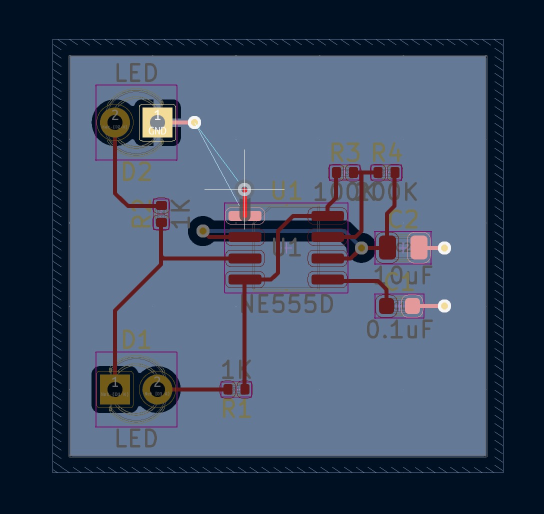
Finished the unfinished routing with the GND via and finally finished all the traces as follows...
Run DRC
DRC can find errors in PCBs such as mismatches between schematic and layout, insufficient clearance or shorts, and unconnected traces.
1. Inspect ▶︎ Design Rules Checker.
2. Check the options as shown in the figure below and click Run DRC.
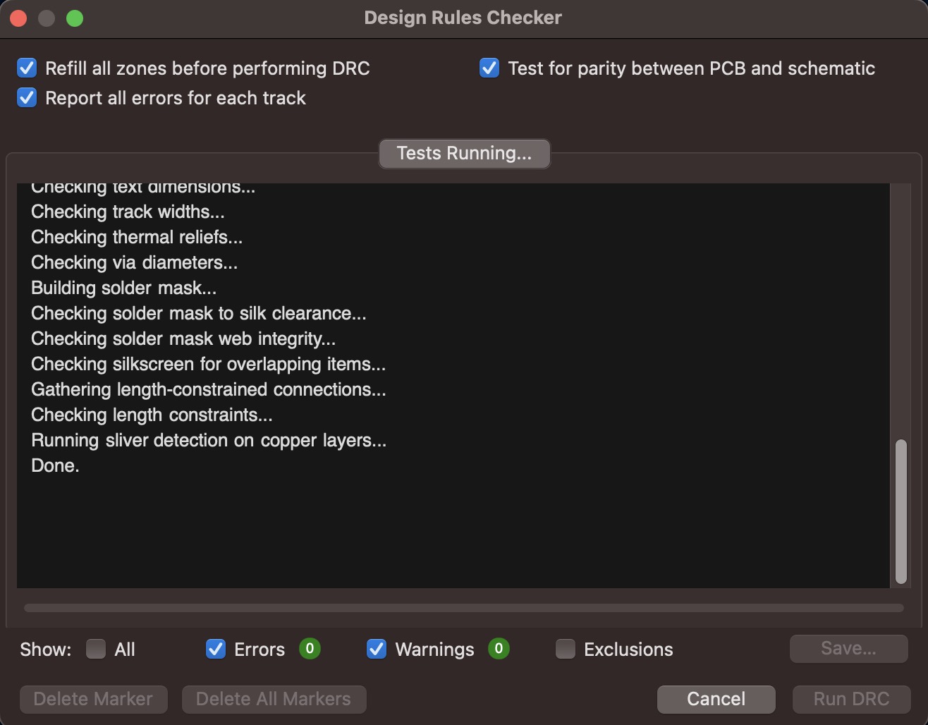
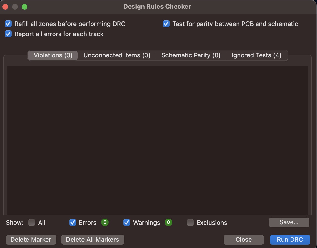
3. After checking, if there is any error, you will see a list of error and warning messages.
4. We completed the entire PCB design without errors and warnings.
View 3D
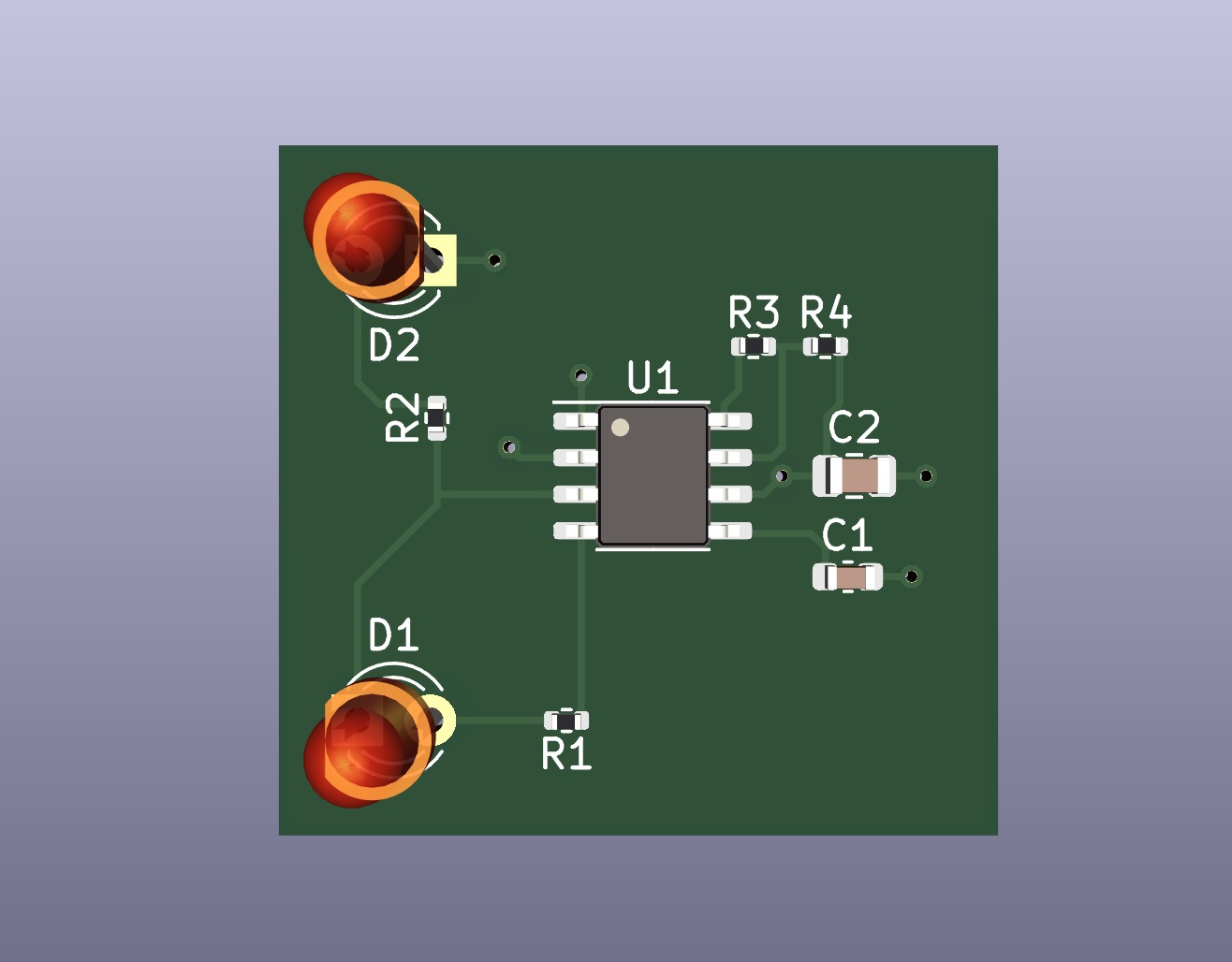
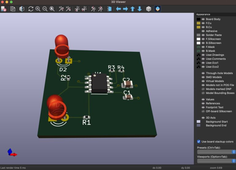
KiCad provides a 3D tool that can be used to check the overall state of a PCB.
Select View ▶︎ View3D.
