KiCad 8 Custom PCB Design Rules
Contents
Introduction
KiCad 8.x’s custom rules feature enables designers to define and apply specific design specifications in board designs, which is useful for advanced design needs such as high-density boards, signal integrity requirements, power or ground planes Special handling, etc.
Install KiCad
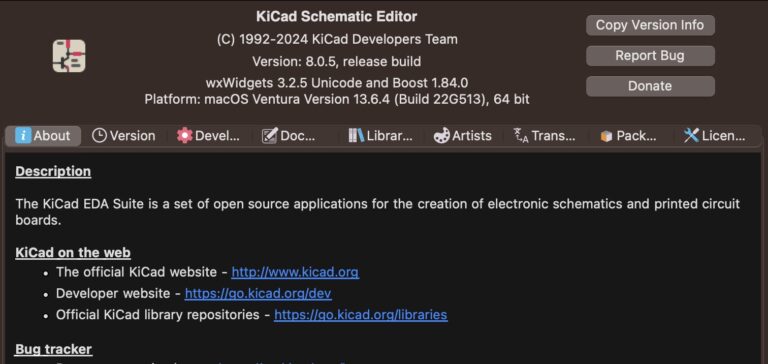
Download KiCad and install it.
Verify installation
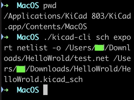
After the installation is complete, open a command line window and enter the following command to confirm whether the KiCad CLI tool is available.
kicad-cli -v8.0.5If you are using macOS, you can go to /Applications/KiCad/KiCad.app/Contents/MacOS/kicad-cli to execute the function.
Custom PCB Rule
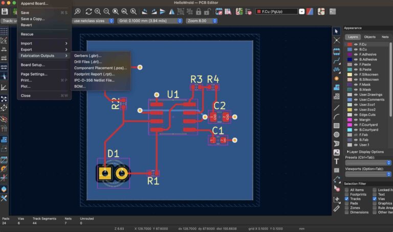
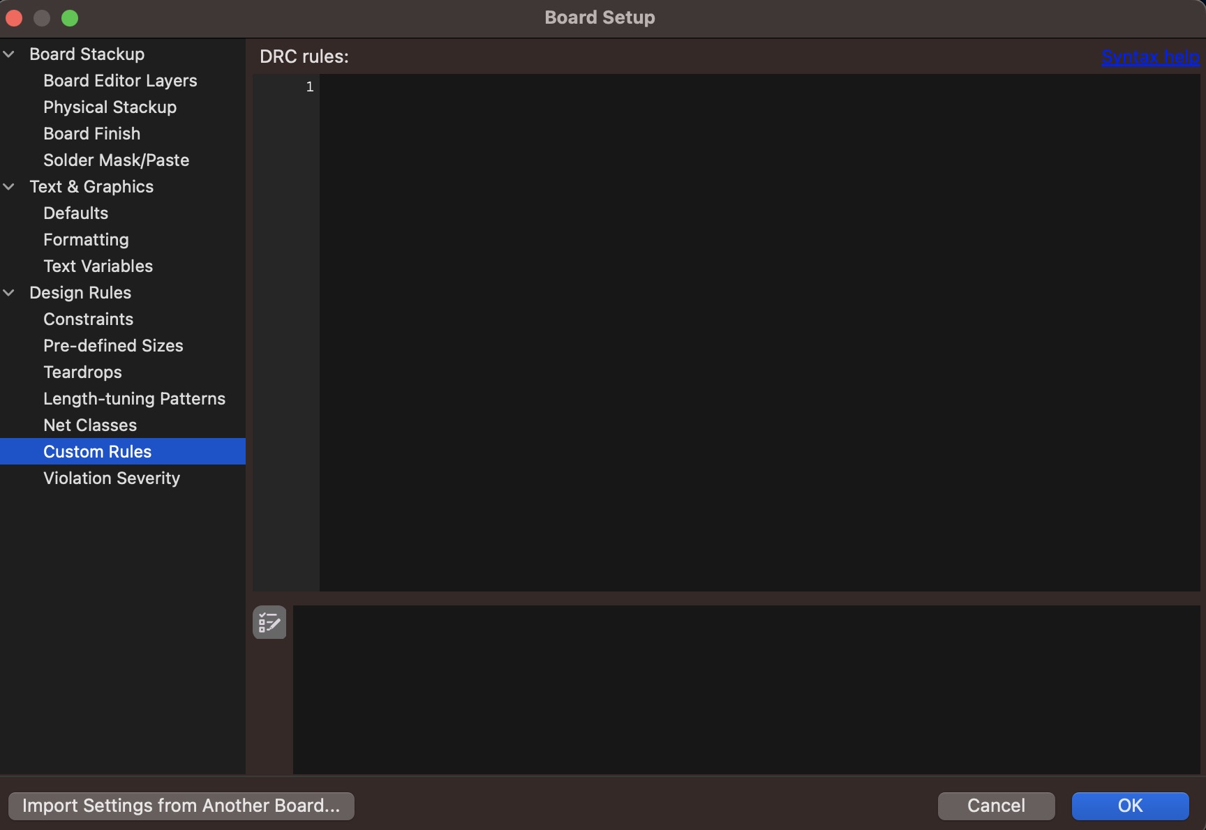
In the PCB design interface, click ▷ File ▷ Board Setup ▷ Design Rules ▷ Custom Rules in the PCB Editor
Rule Syntax Help
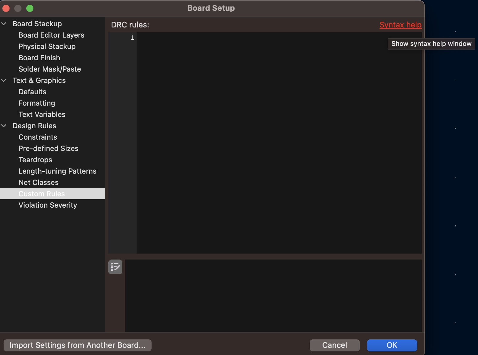
In Board Setup, click "Syntax help" in the upper right corner.
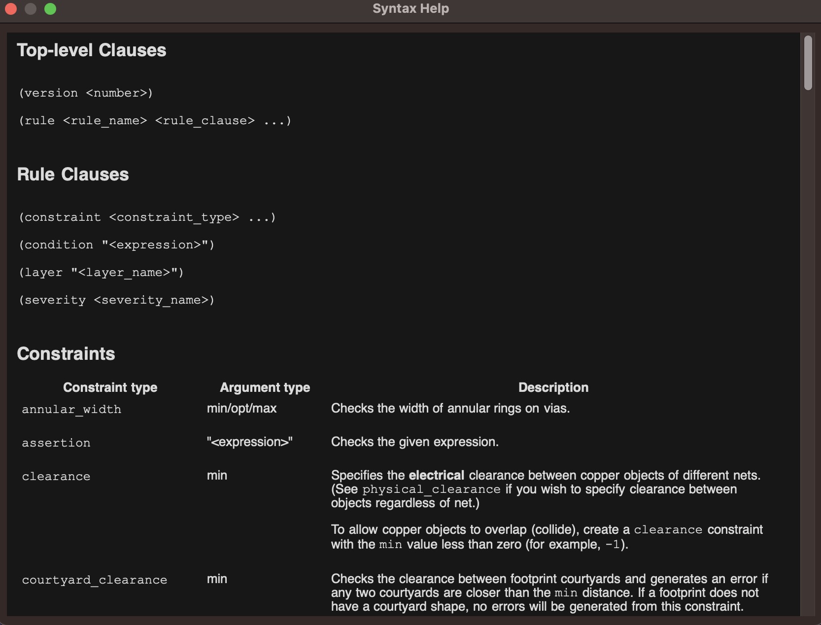
Rule Conditions And Constraints
Condition: Define the object to which the rule applies. For example, apply rules to a specific type of trace, via, or component. Conditions use attributes (such as traces, vias, pad types, attributes) to specify the application scope.

Constraint: Define specific constraints, such as minimum spacing, maximum trace width, etc. You can specify a variety of constraints to control different design parameters.
(version 1)
(rule "MyCustomRule"
    (condition "A.Type == 'track' && A.NetClass == 'Power'")
    (constraint clearance (min 0.5mm)))
Add A New Rule
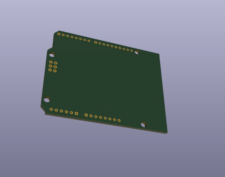
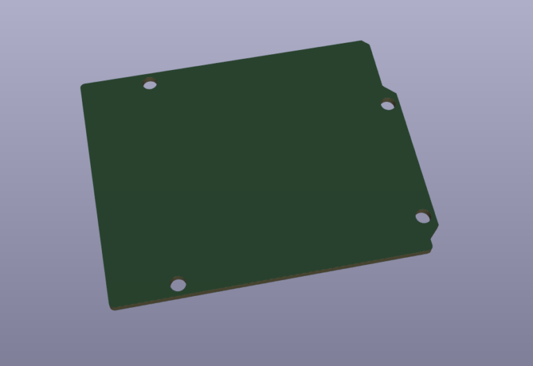
Using the custom_pads_test.kicad_pcb sample file in KiCad 8 to illustrate how to apply custom design rules, here are the steps and examples.
1. Open the Demo file
Load the PCB file project "custom_pads_test.kicad_pro". (This file is usually located in KiCad's demo project folder.)
2. Add custom rules "MyTrack"
Click custom_pads_test.kicad_pcb and enter PCB Editor and select ▷ File ▷ Board Setup ▷ Design Rules ▷ Custom Rules
(version 1)
(rule "MyTrack"
    (condition "A.Type == 'track'")
    (constraint track_width (max 0.1mm)))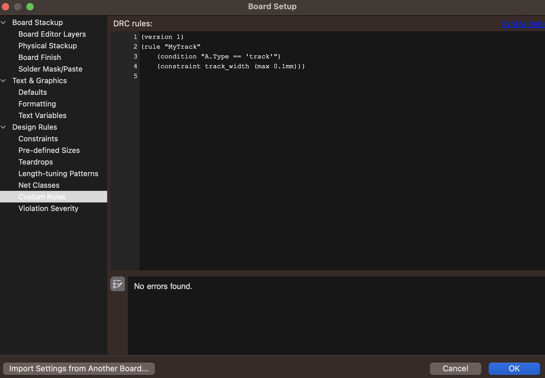
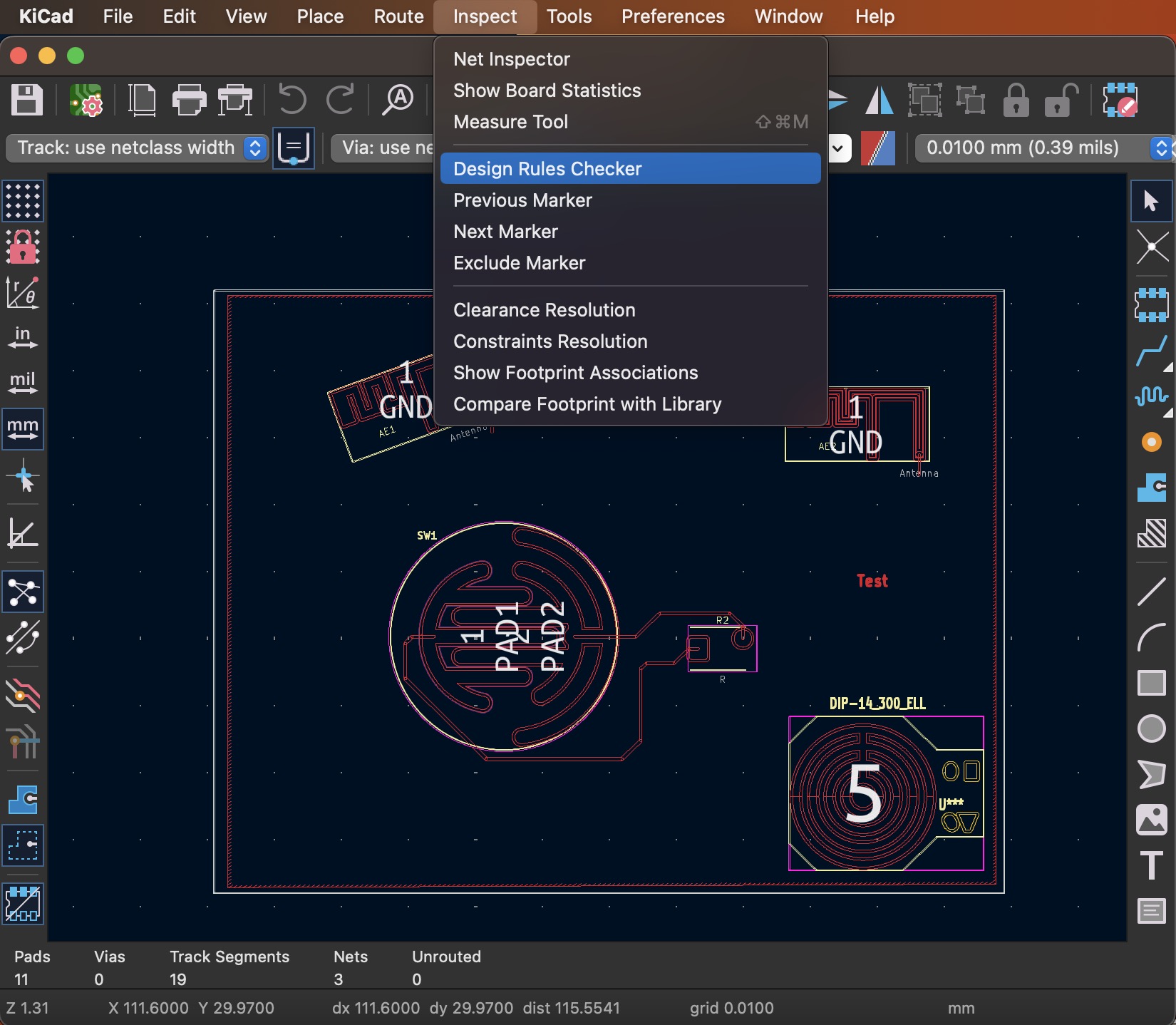
Run DRC
Click Inspect ▷ File ▷ Design Rules Checker
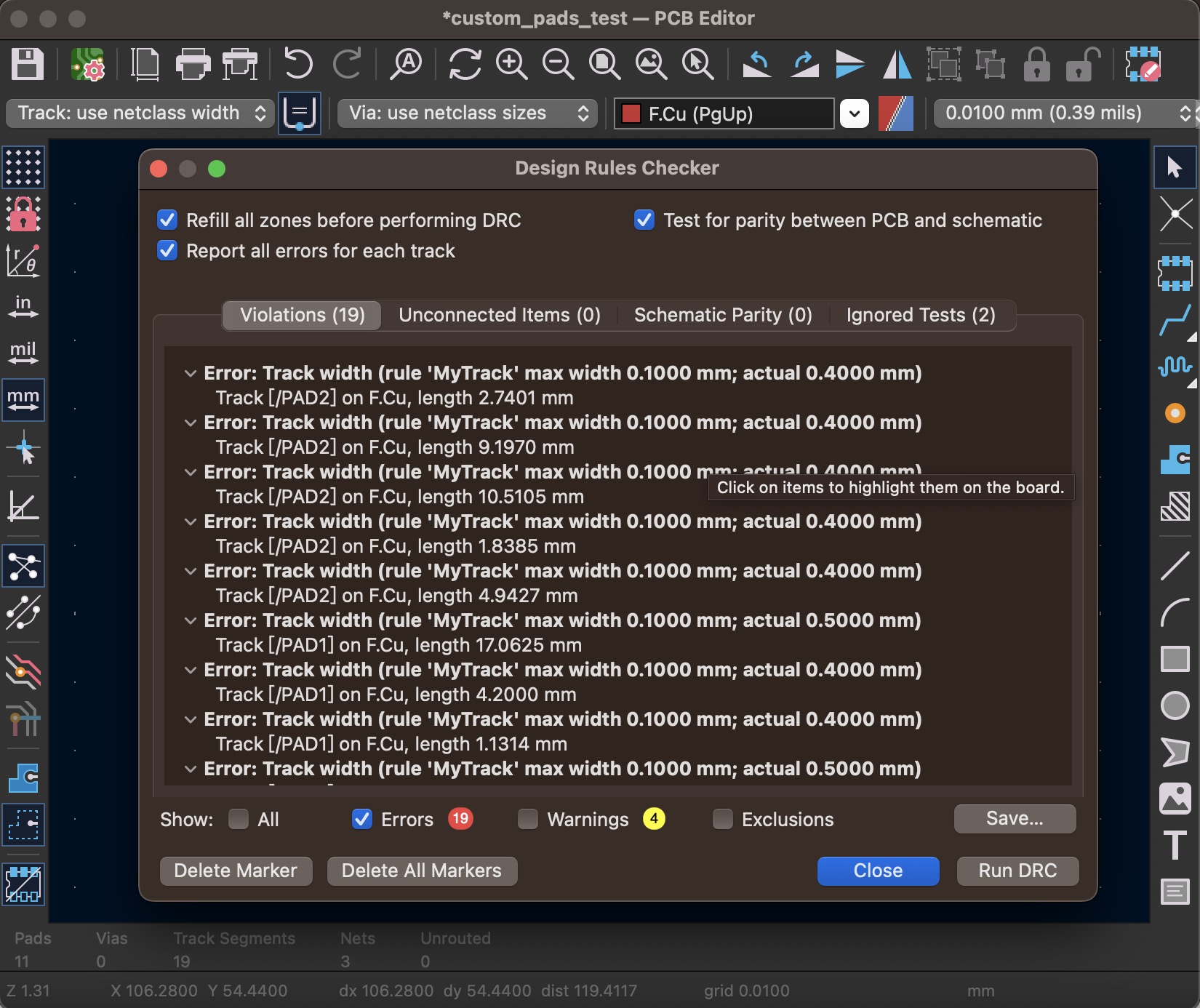
Set as follows and click "Run DRC".
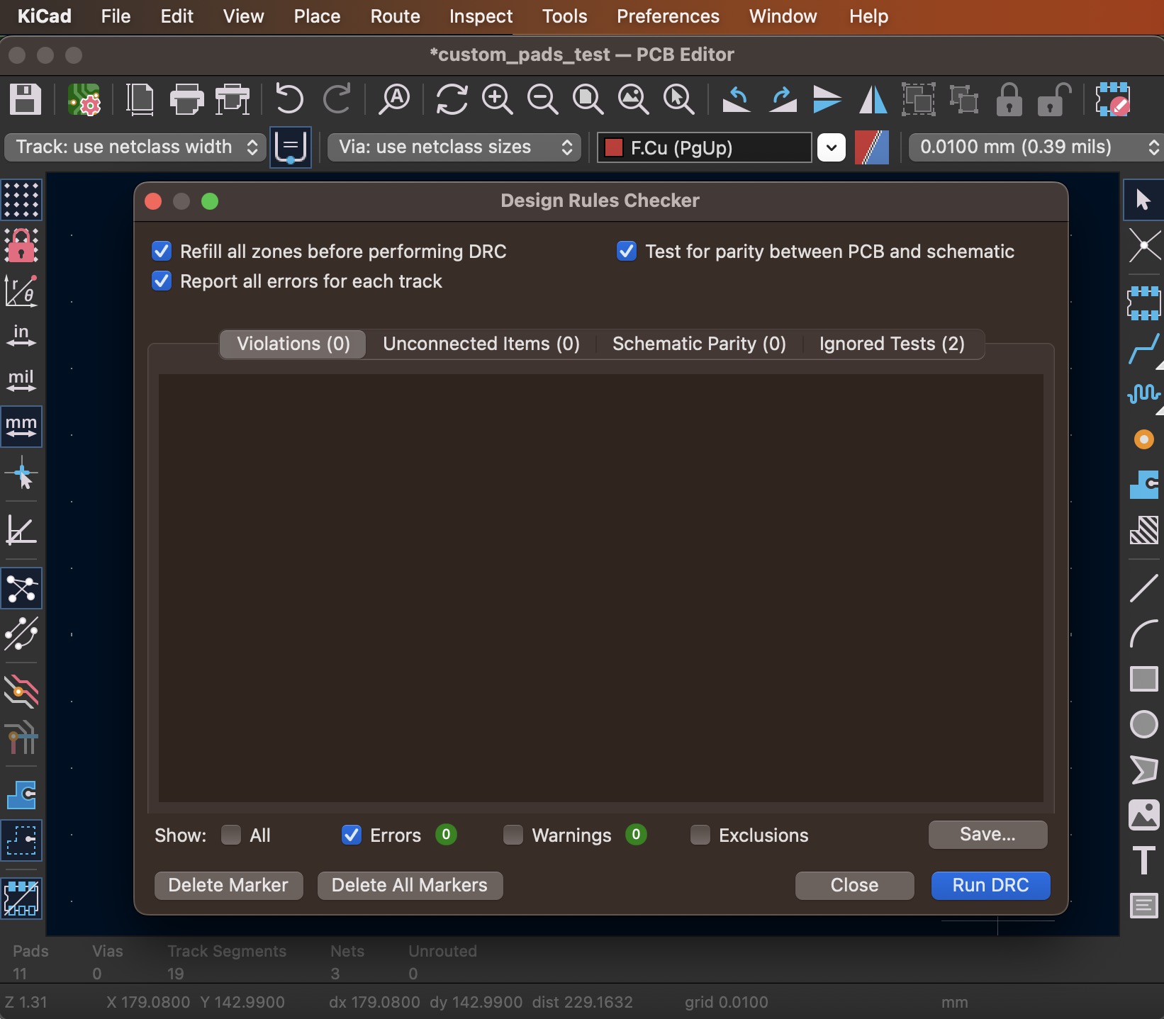
DRC Results For MyTrack Rule
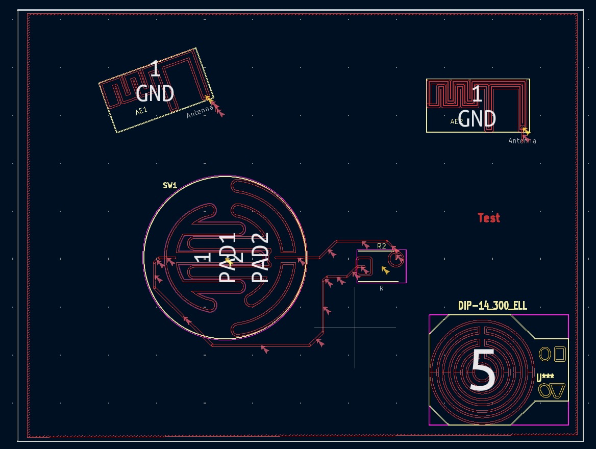
There are 19 errors in Violations that are affected by MyTrack rules.
Click "Close" .
Conclusion
KiCad's custom rules feature provides highly flexible design control, allowing engineers to design different rules based on specific needs, thereby achieving more precise and customized PCB designs. By defining conditions and constraints, design elements such as traces and vias can be effectively managed to improve design quality and reliability.
