KiCad 8 Tutorial – Design Circuit
Contents
Create a HelloWorld Project
Run KiCad 8.x App, Select File ▶︎ New Project ▶︎ Type "HelloWorld" and finish as shown below...
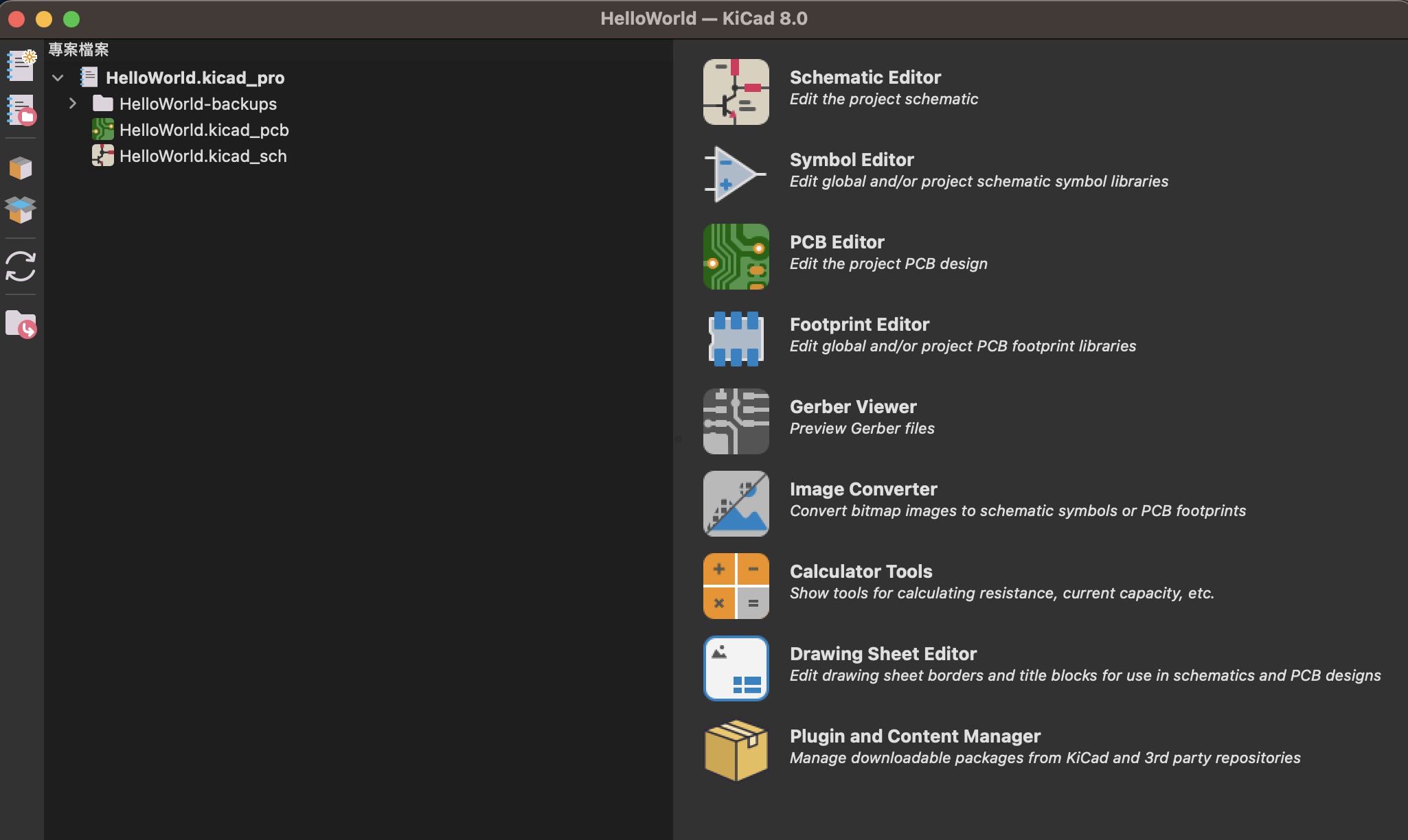
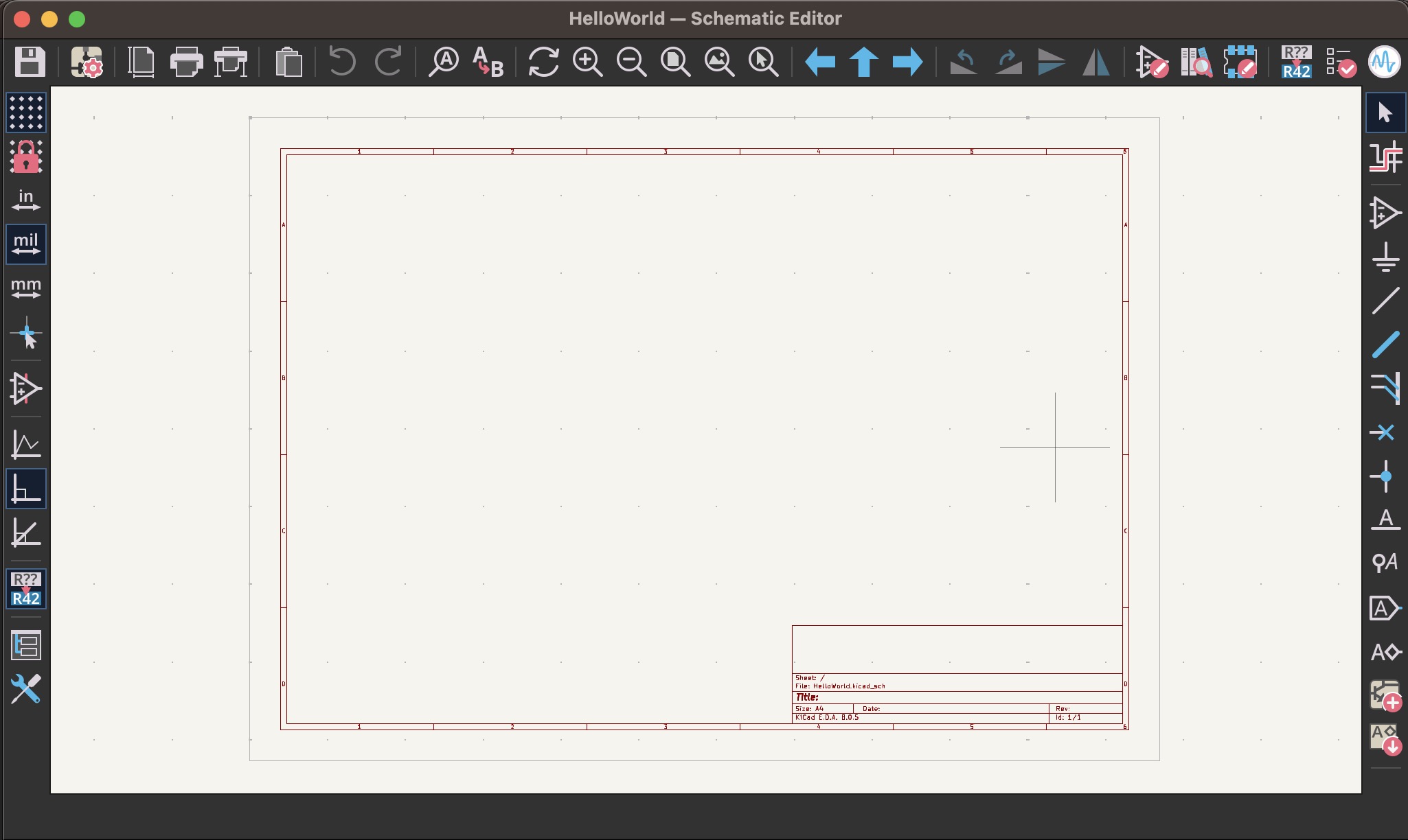
Double click on "HelloWorld.kicad_sch" will open the "Schematic Editor" as shown below...
Add Component Symbol
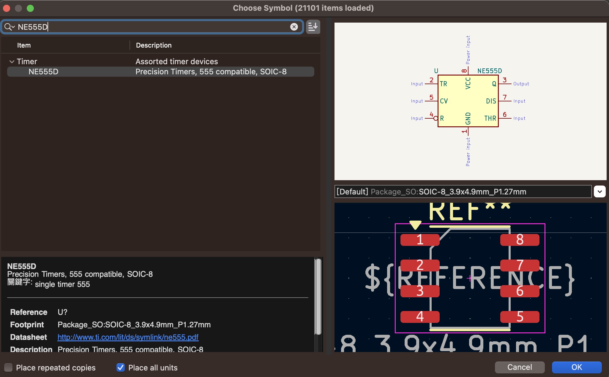
1. Select Place ▶︎ Add Symbol ▶︎ Type "timer" ▶︎ Select "NE555D" ▶︎ Click "OK".
2. Place the component into the drawing area.
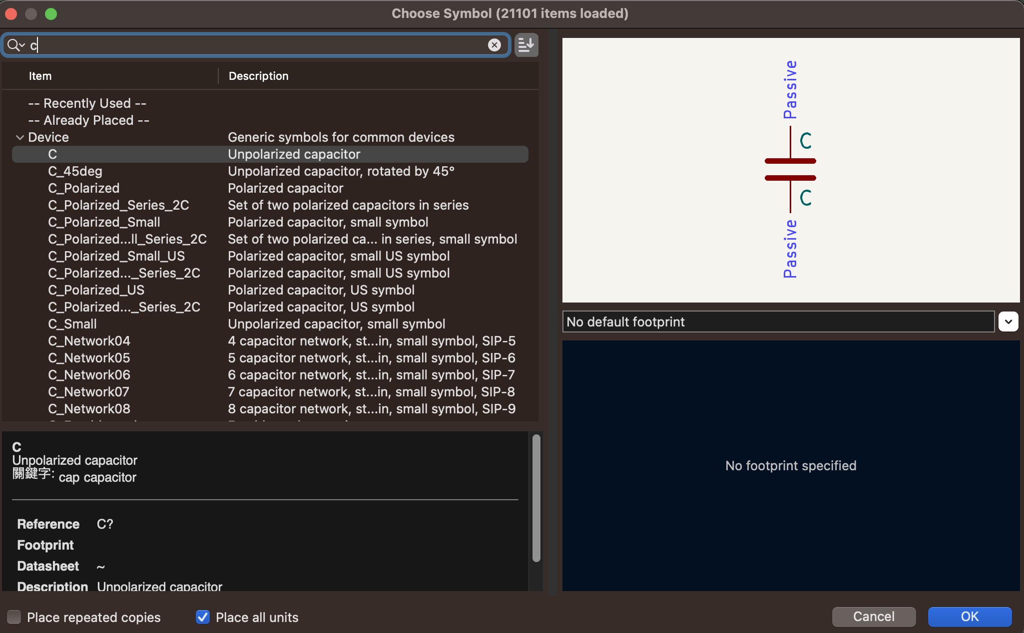
1. Select Place ▶︎ Add Symbol ▶︎ Type "b" ▶︎ Select "C" ▶︎ Click "OK".
2. Repeat the placement once and place the component in the drawing area.
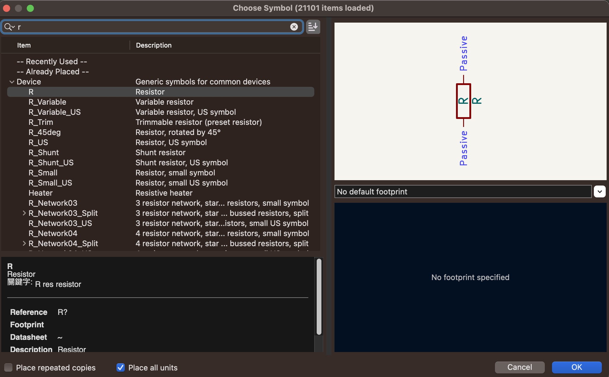
1. Select Place ▶︎ Add Symbol ▶︎ Type "r" ▶︎ Select "R" ▶︎ Click "OK".
2. Repeat the placement 4 times and place the component in the drawing area.
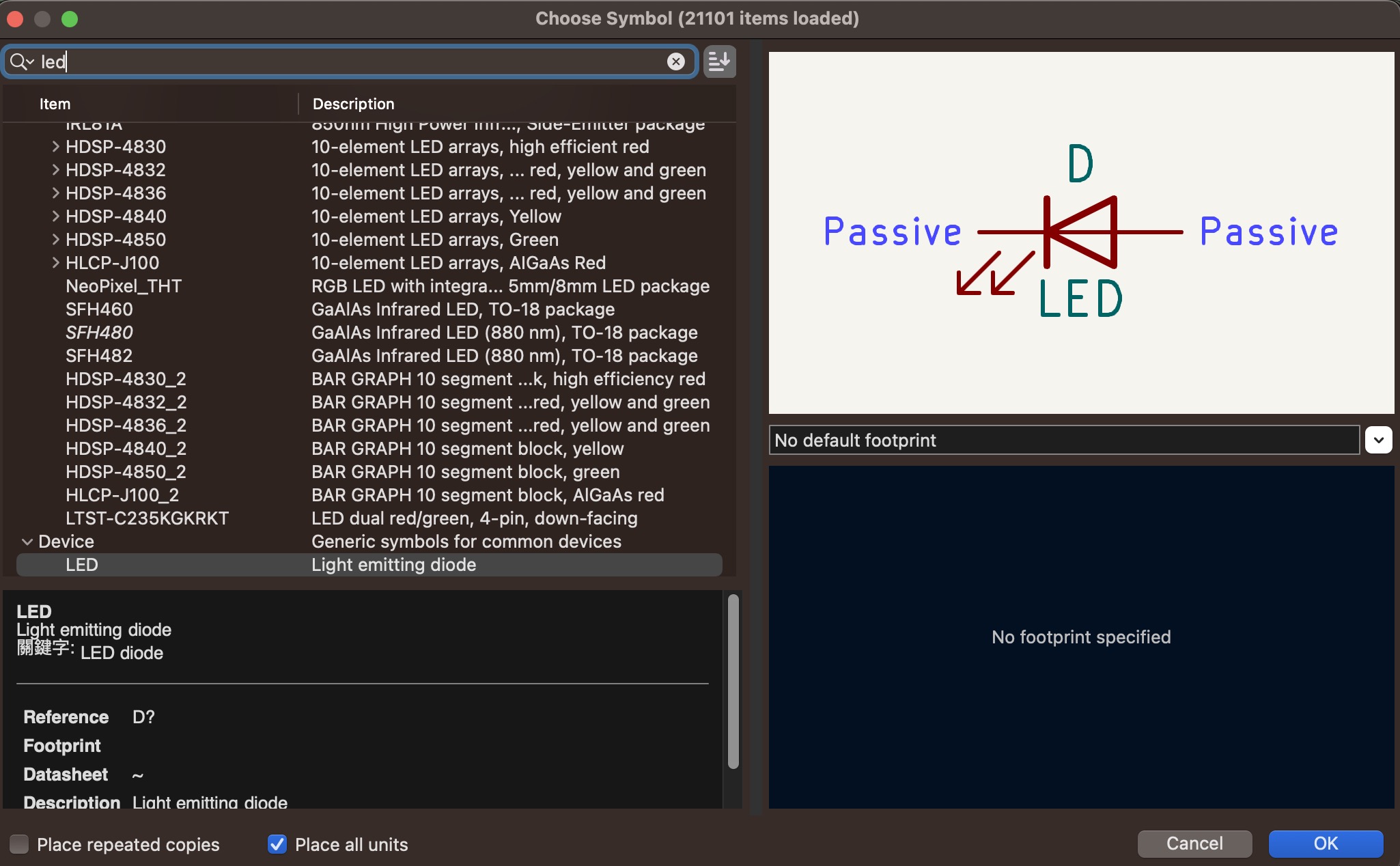
1. Select Place ▶︎ Add Symbol ▶︎ Input "led" ▶︎ Select "LED" ▶︎ Click "OK".
2. Repeat the placement 2 times and place the component in the drawing area.
1. Add "Power" and "Ground" symbols.
2. Select Place ▶︎ Add Power ▶︎ Input "9" ▶︎ Select "+9V" ▶︎ Click "OK".
3. Place components into the drawing area.
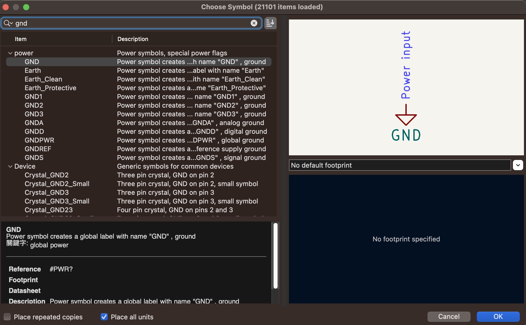
4. Select Place ▶︎ Add Power ▶︎ Enter "g" ▶︎ Select "GND" ▶︎ Click "OK".
5. Place components into the drawing area.
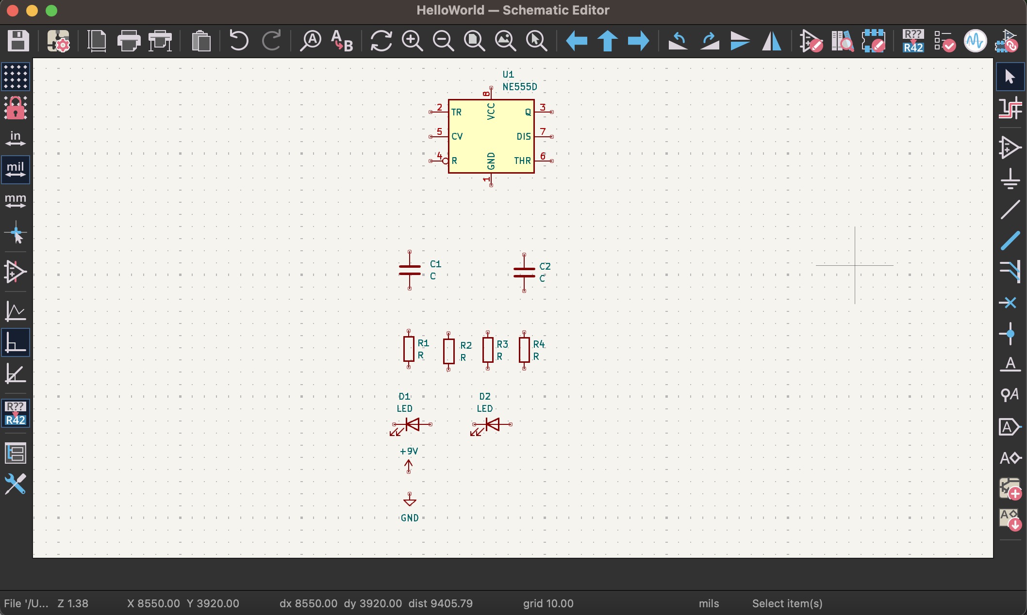
All components are placed as shown below...
Arrange Related Components
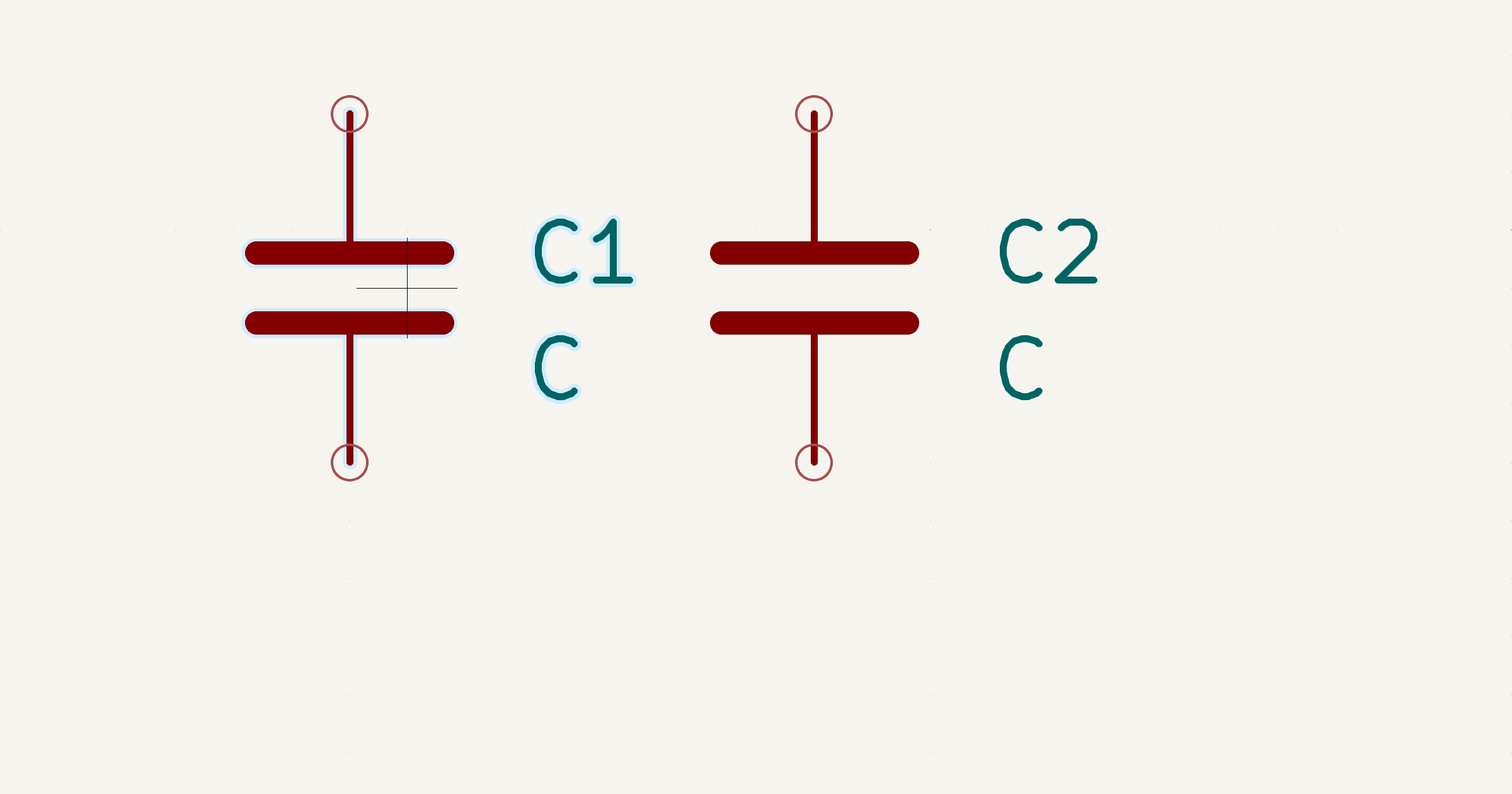
Select the component you want to move such as C1 (it will be highlighted) ▶︎ Press the keyboard "m (move) or d (drag)" ▶︎ Move the mouse to move or drag the component.
Arranging elements can roughly look like this...
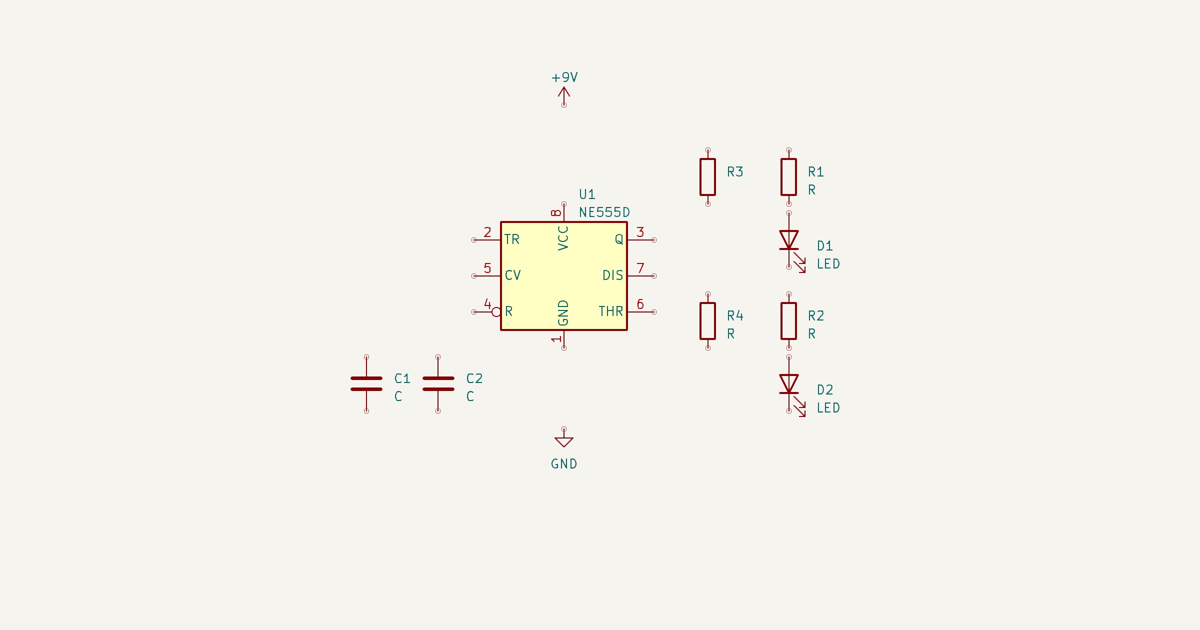
Pull a Wire From a Component’s Pin
First select the "pin-point" of the component to be connected or select Place ▶︎ Add Wire At this moment the mouse will "change" as shown below...
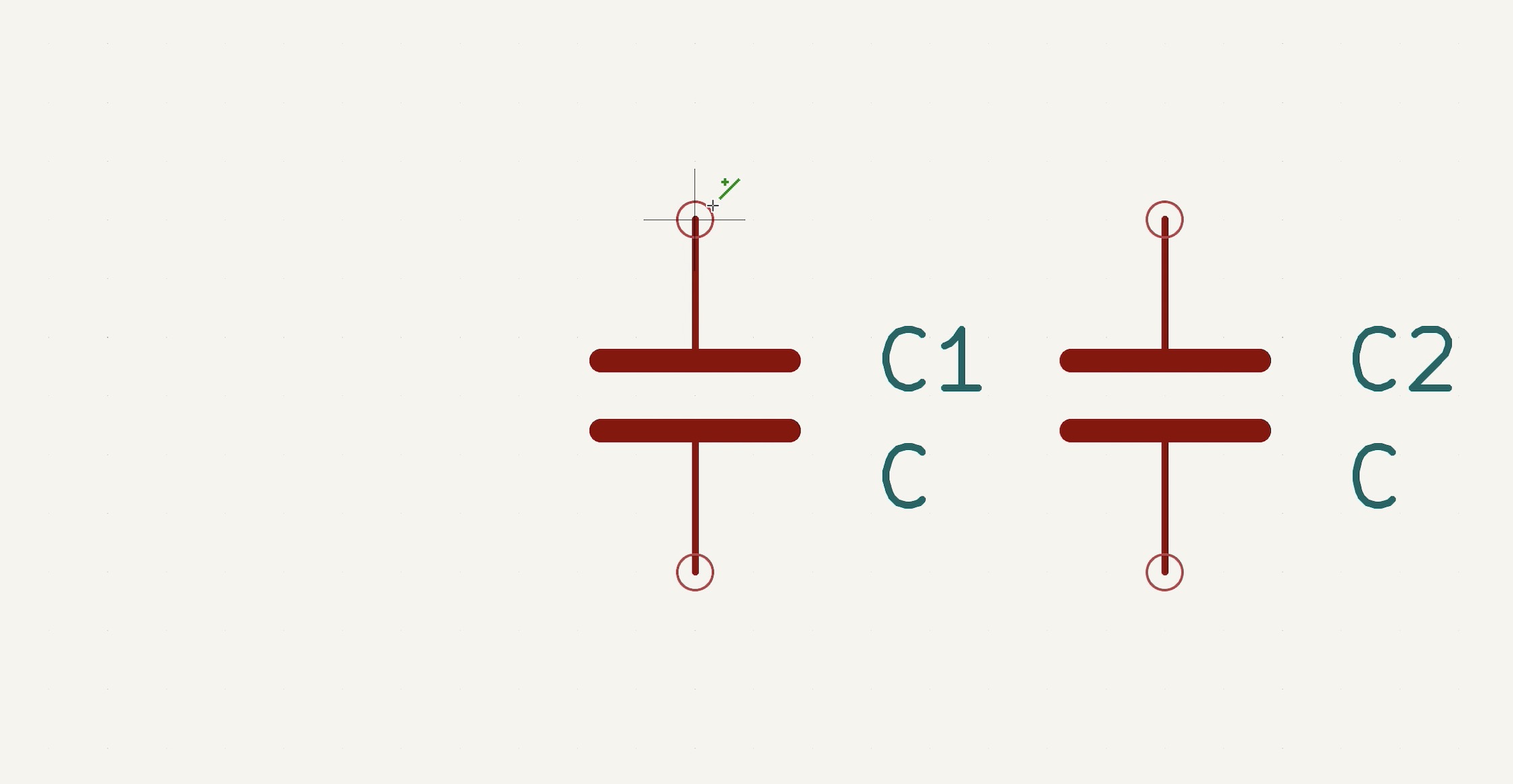
Click to drag the mouse and pull out a wire, as shown below...
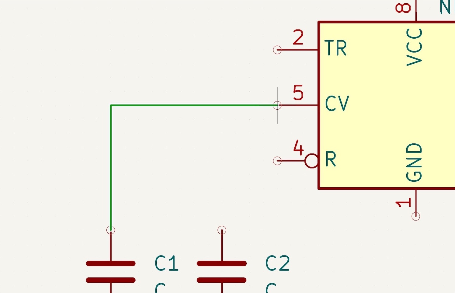
Complete the following connections in this way, as shown below...
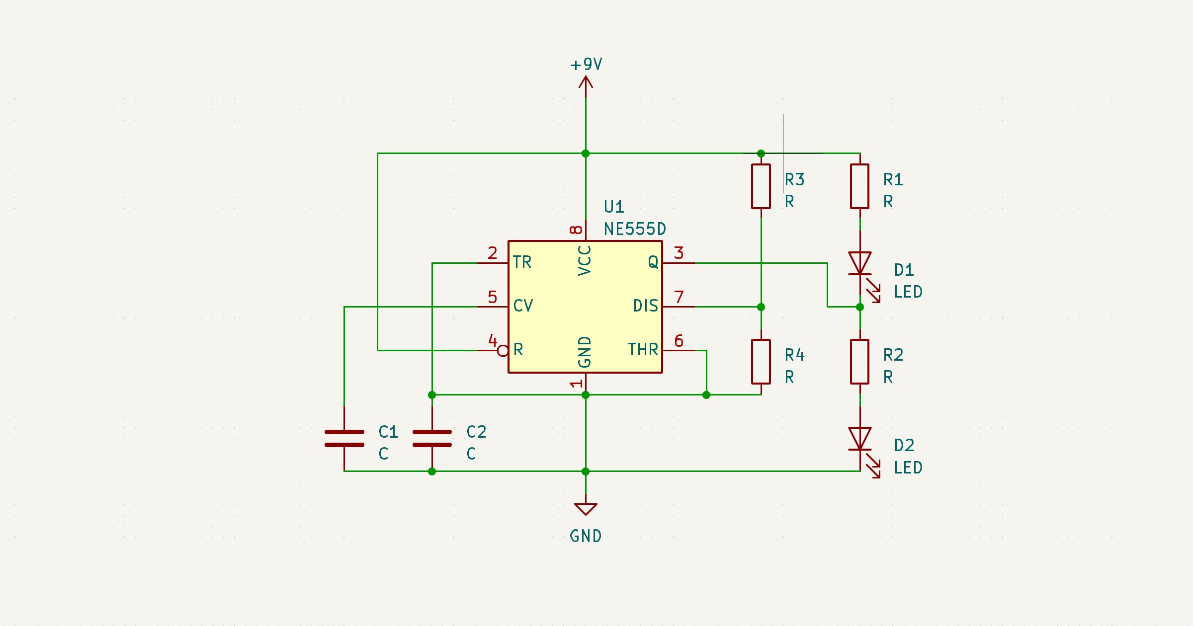
Modify Component Value
Select a component R1 (it will be highlighted) ▶︎ Press keyboard "e (Properties...)" ▶︎ Type "1K" in the Value field.
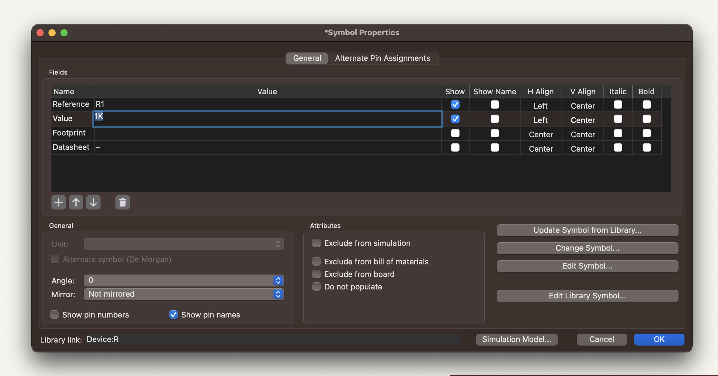
You need to change component value can be done in this way as below...
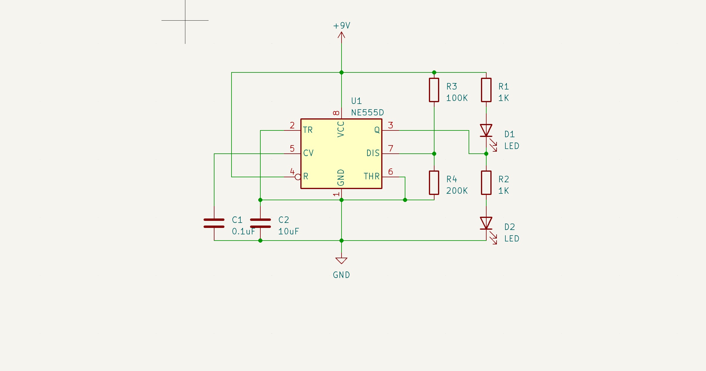
Check KiCad Circuit
Delete unnecessary connection points ▶︎ "+" cursor moves to the node to be deleted ▶︎ Click the right mouse button ▶︎ Select "Delete"
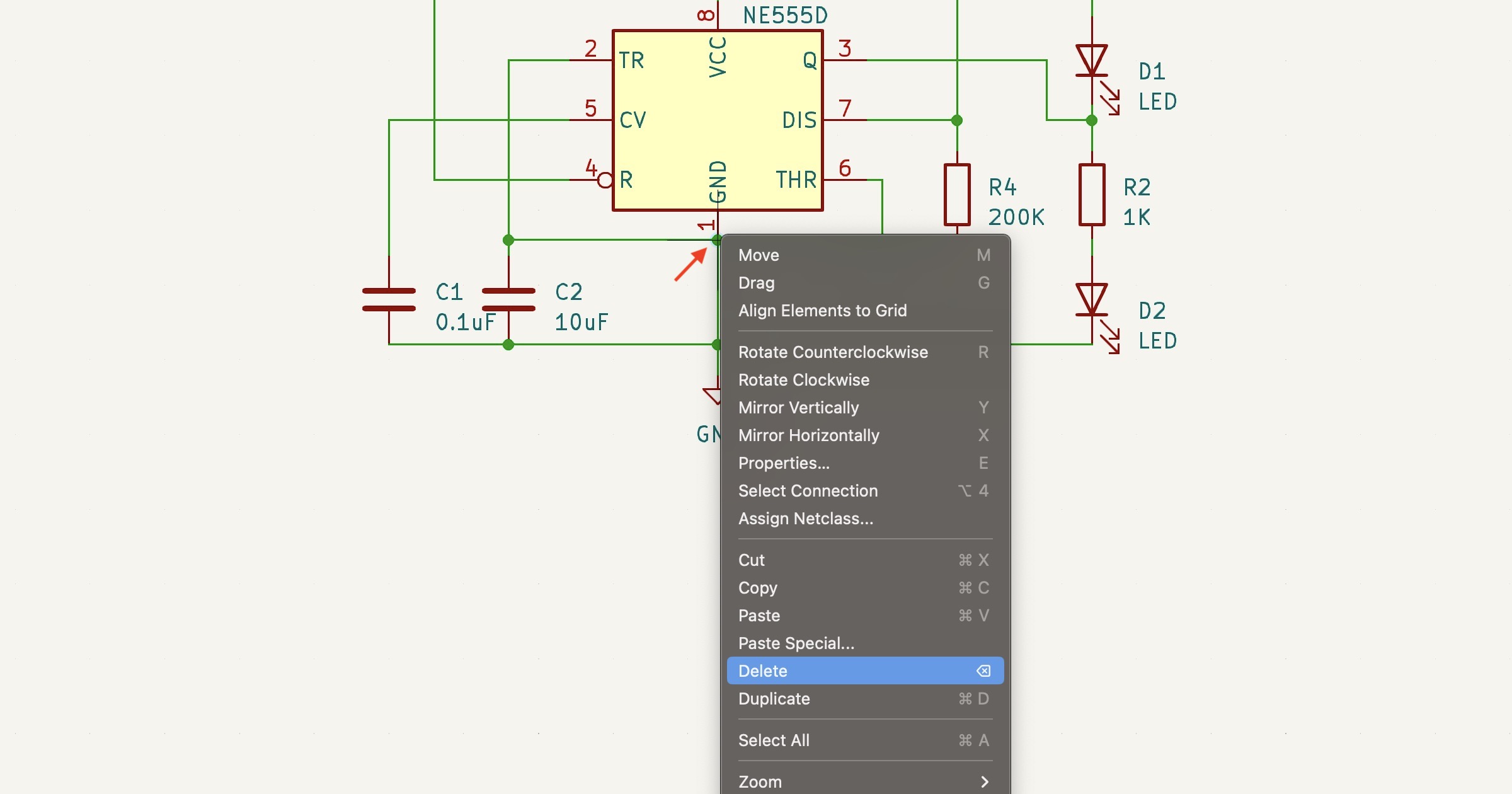
Finally complete the following circuit design
Run ERC and Correct Problems
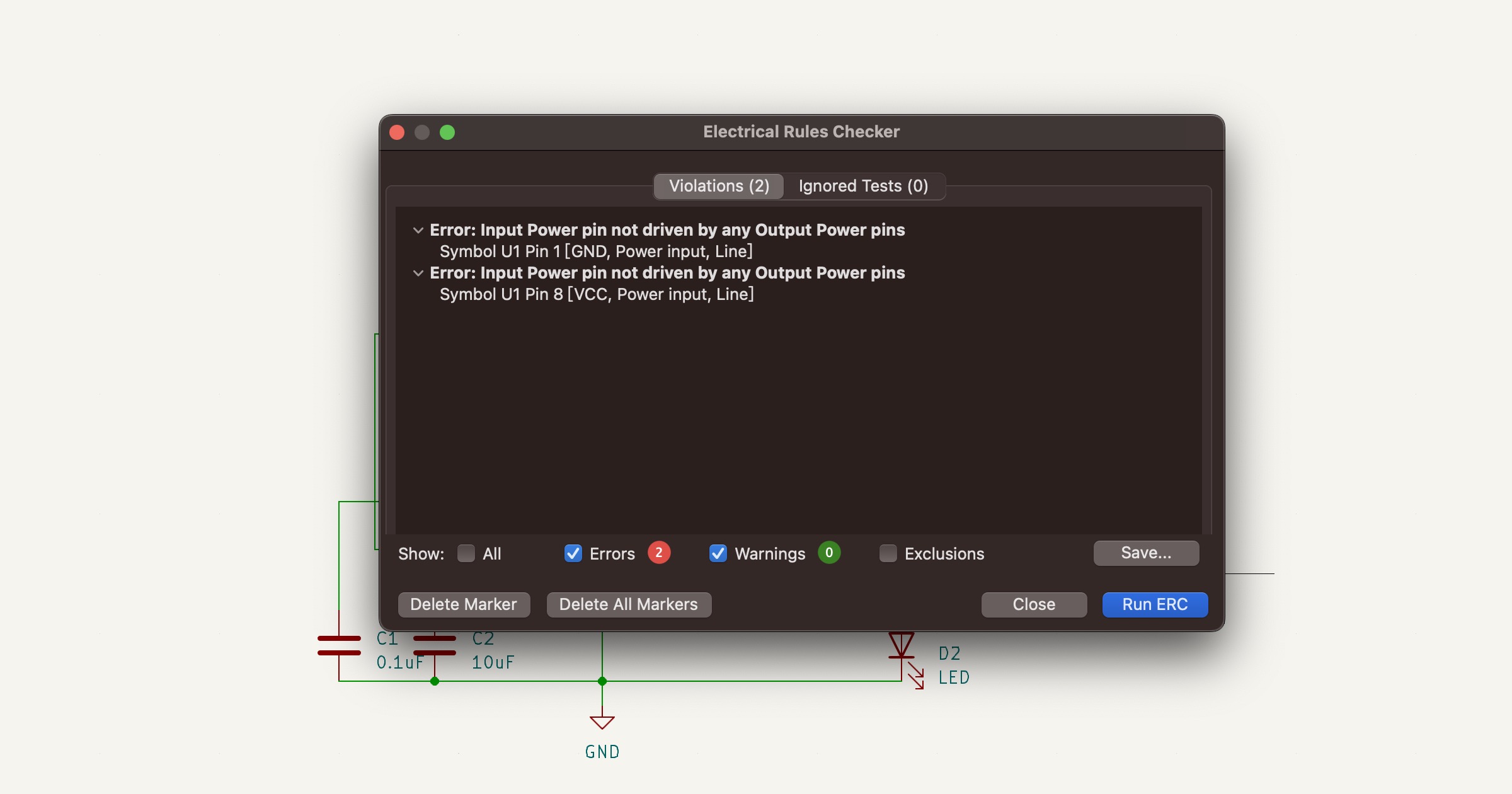
1. Select Inspect ▶︎ Click "Electrical Rules Checker" ▶︎ Click "Run ERC".
2. There will be two errors ▶︎ Click "Close", as shown below...
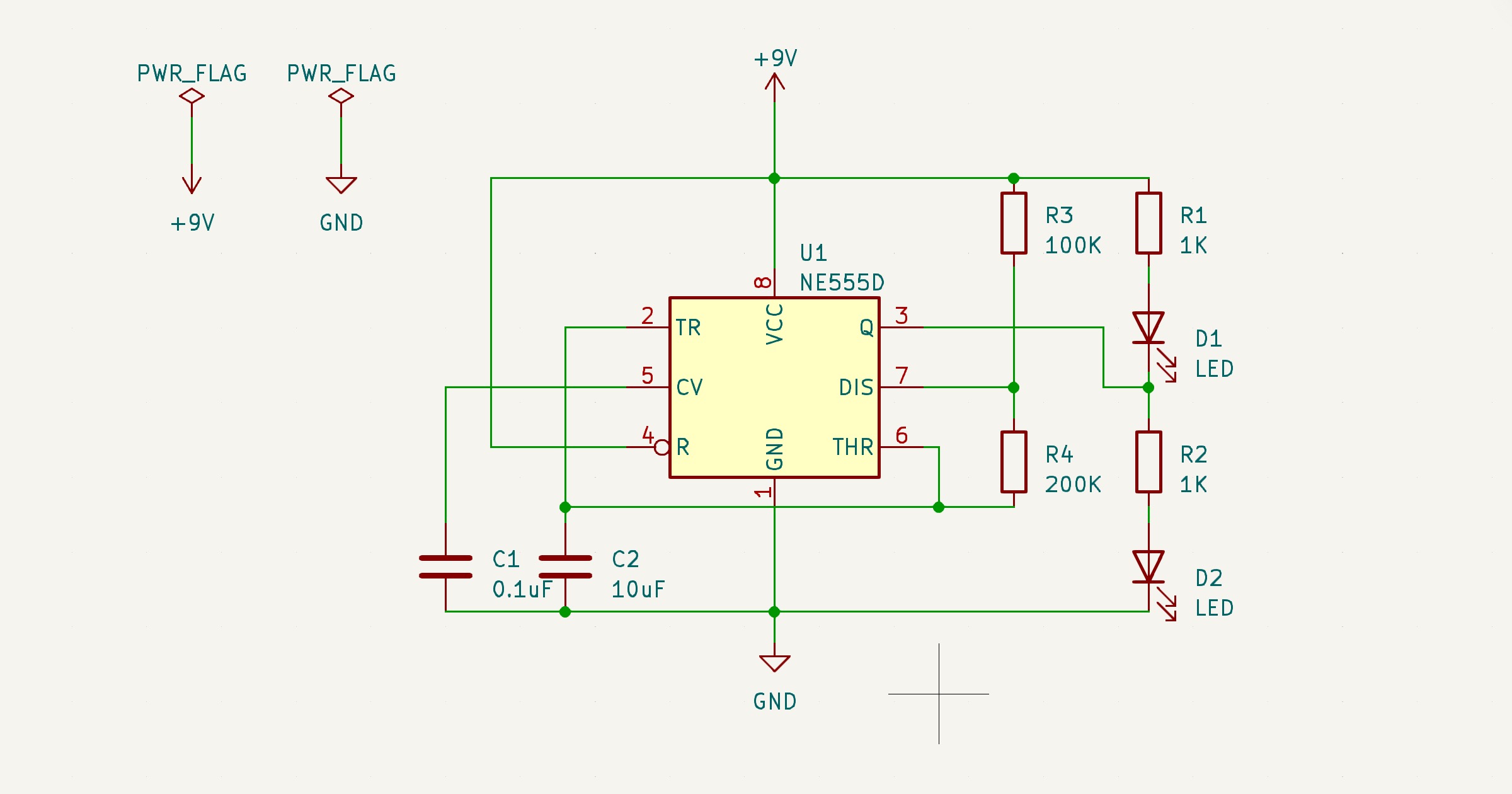
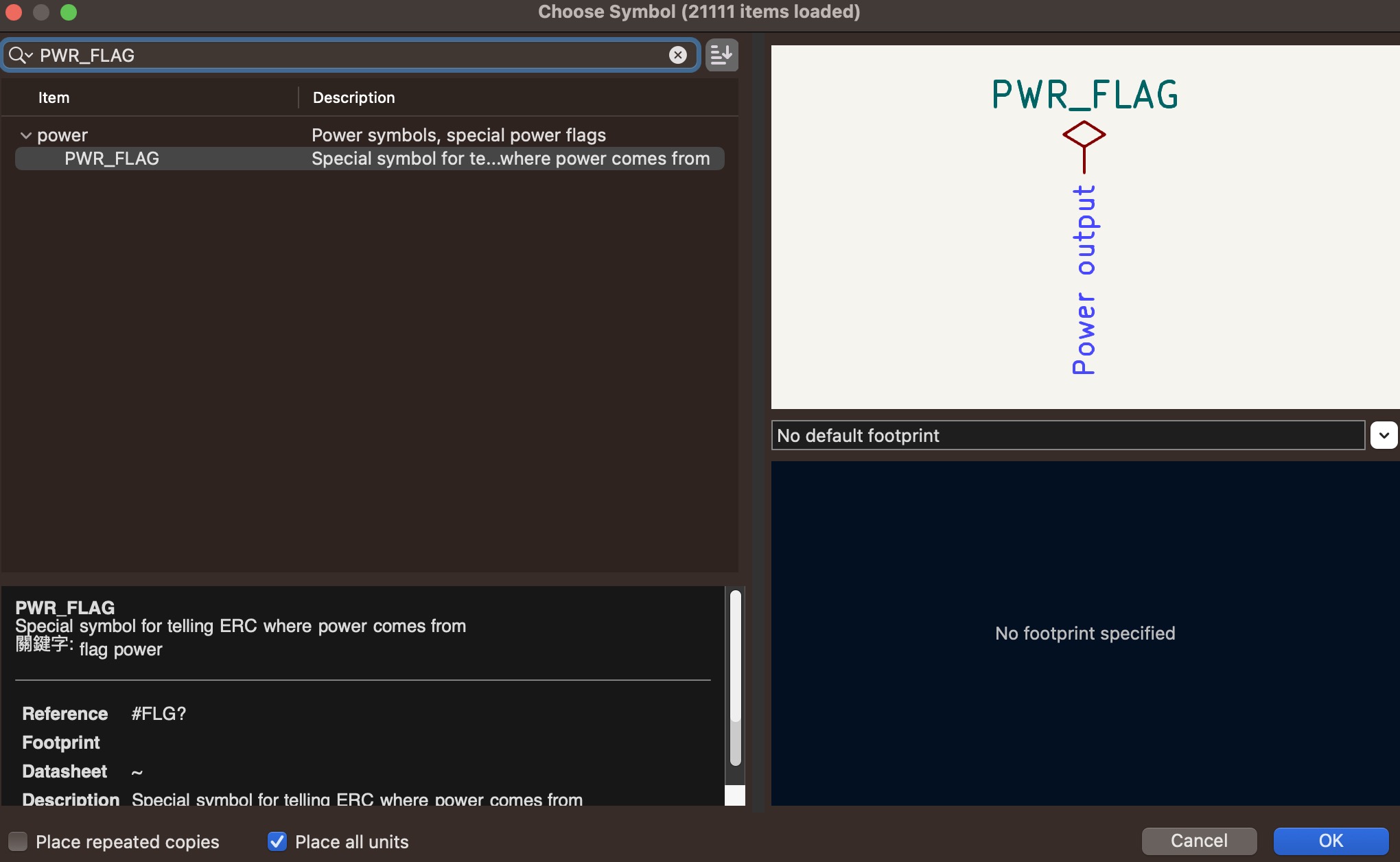
1. Add "PWR_FLAG" symbol.
2. Select Place ▶︎ Add Power ▶︎ Enter "pwr" ▶︎ Select "PWR_FLAG" ▶︎ Click "OK".
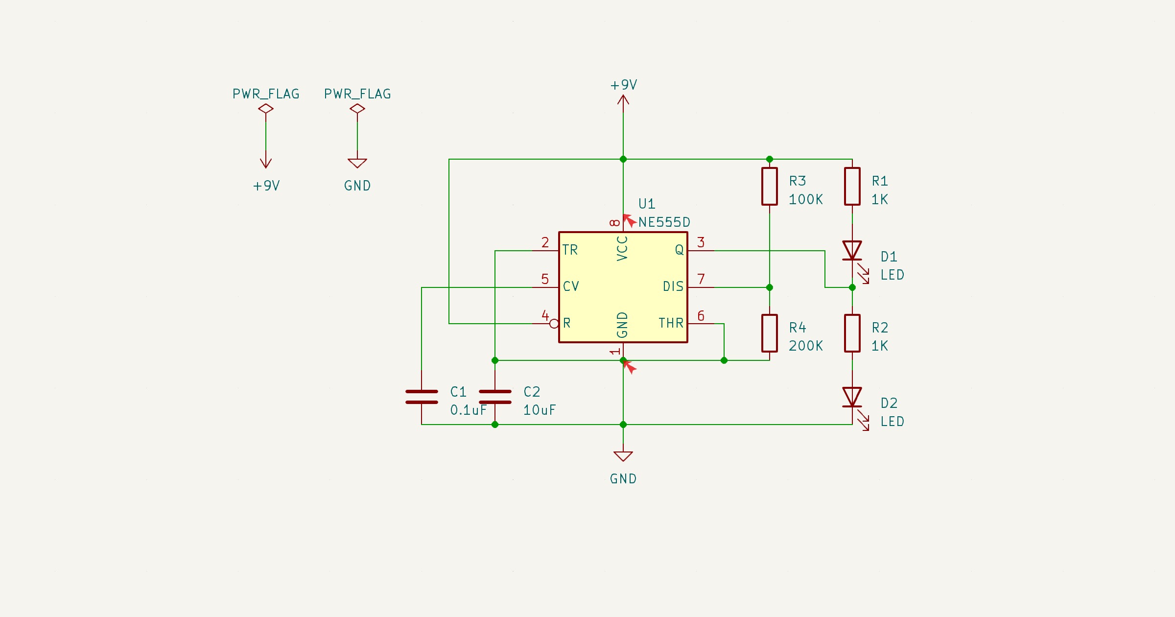
3. Repeat 2 times and place PWR_FLAG in the drawing area, as shown below...
1. Add a set of "+9V" and "GND" symbols to the drawing area again, and you can press "r" to rotate the symbols.
2. And complete the following connections as shown below...
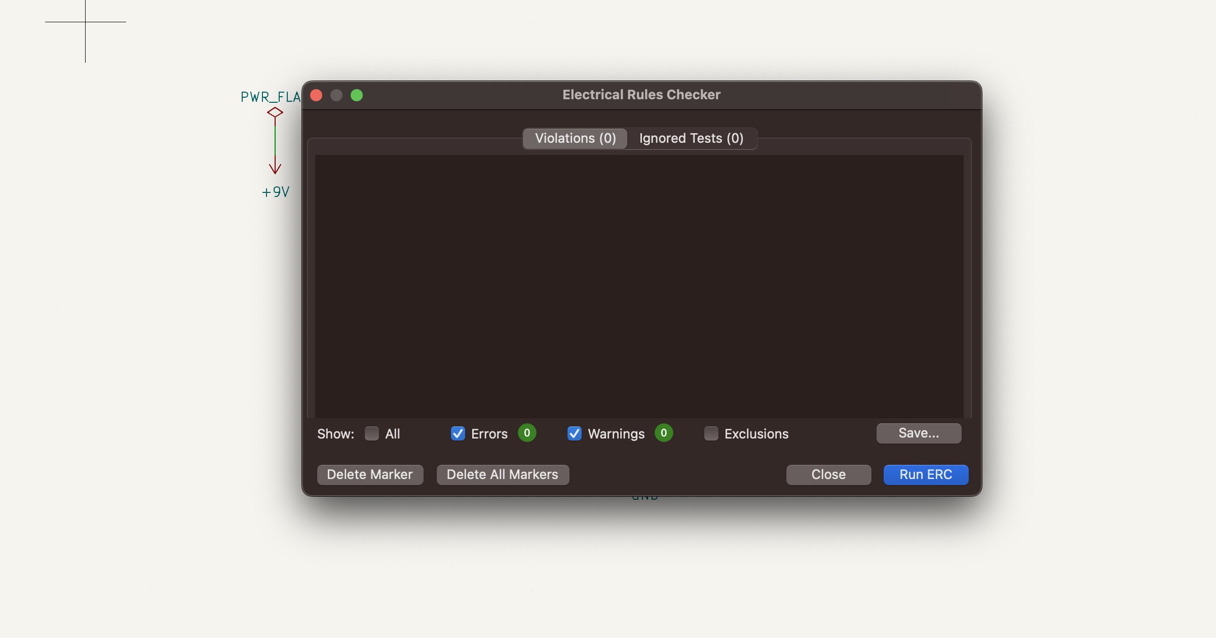
1. Select "Electrical Rules Checker" again ▶︎ Click "Run ERC".
2. Will get Errors = 0 and Warnings = 0.
Complete the circuit design.

Note : Modify or Re-Annotate Part Number
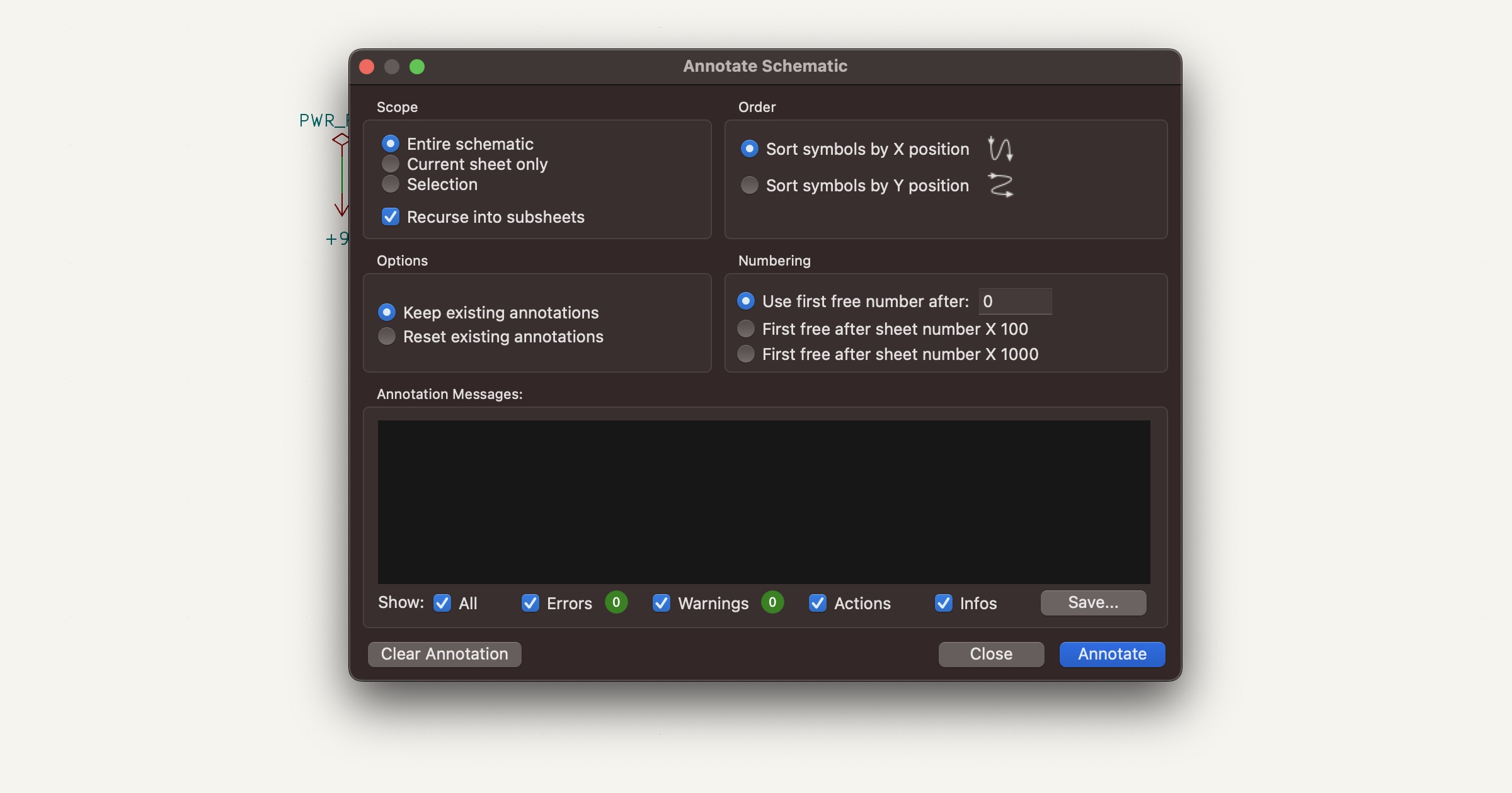
⚑ After KiCad V7.x or V8.x, component numbers such as R1, R2, R3, R4, C1, ... will be automatically generated when new symbols are added. For KiCad V6.x, the component number is "R?", so it is necessary to execute "Annotate Schematic" to generate the component number.
⚑ Select Tools ▶︎ Click "Annotate Schematic" ▶︎ Click "Annotate".
