KiCad 8.x Tutorial – Tip Transparent
Contents
Introduction
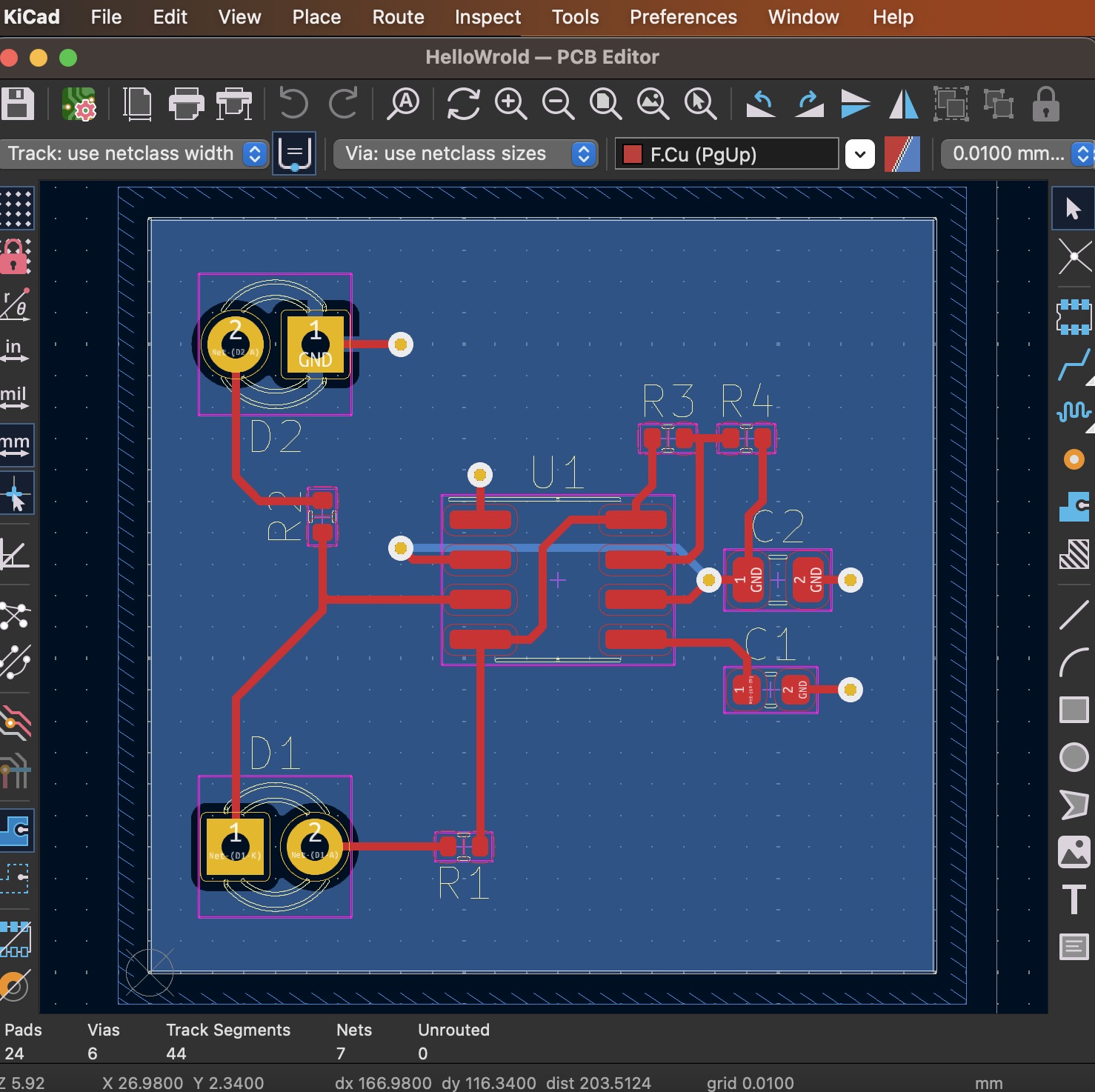
In KiCad 8.x, you can use transparency to improve the appearance and readability of your PCB designs. Features that use transparency in KiCad 8.x include traces, borders, fills, screens, and pads.
Prepare A KiCad Project File
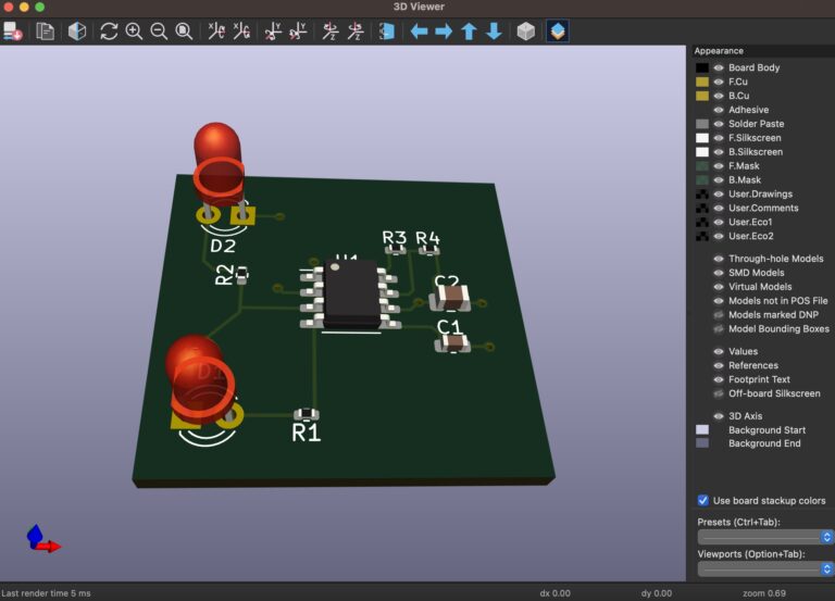
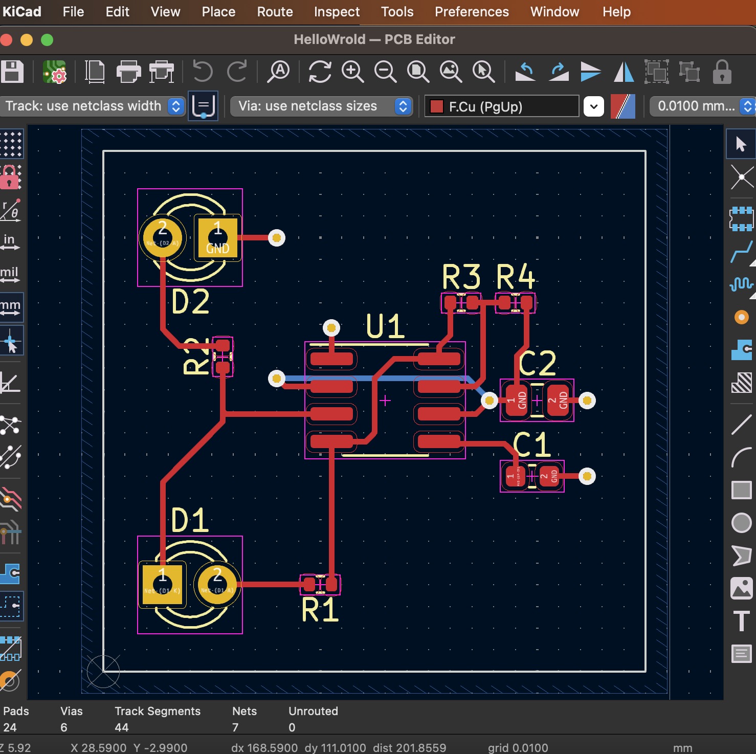
Prepare a KiCad Project (containing Schematic and PCB files).
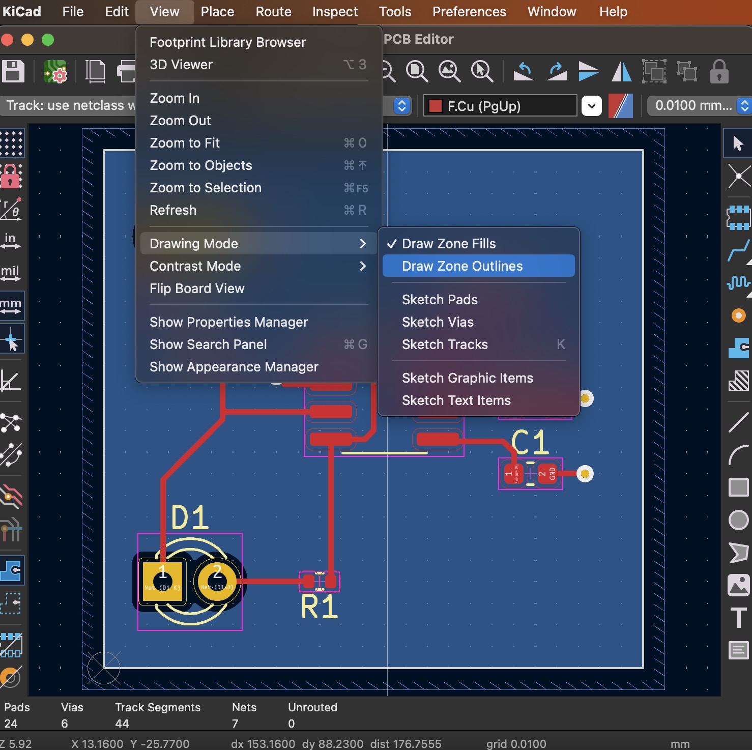
KiCad 8.x’s Zone Outlines.
View ▷ Drawing Mode ▷ Draw Zone Outlines
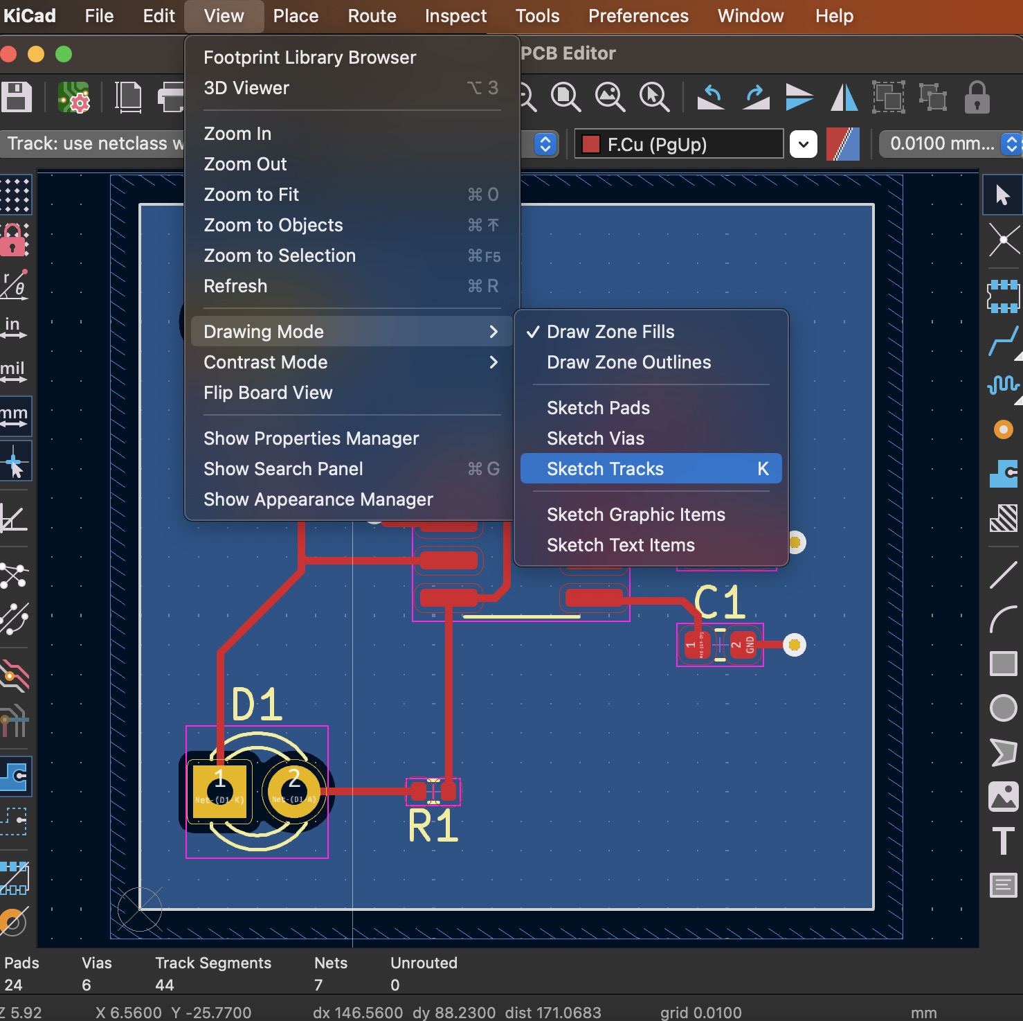
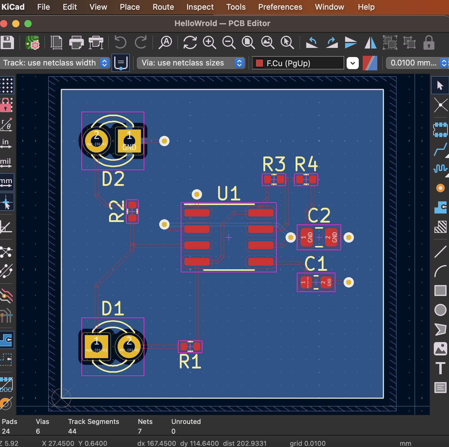
KiCad 8.x’s Sketch Tracks
View ▷ Drawing Mode ▷ Sketch Tracks
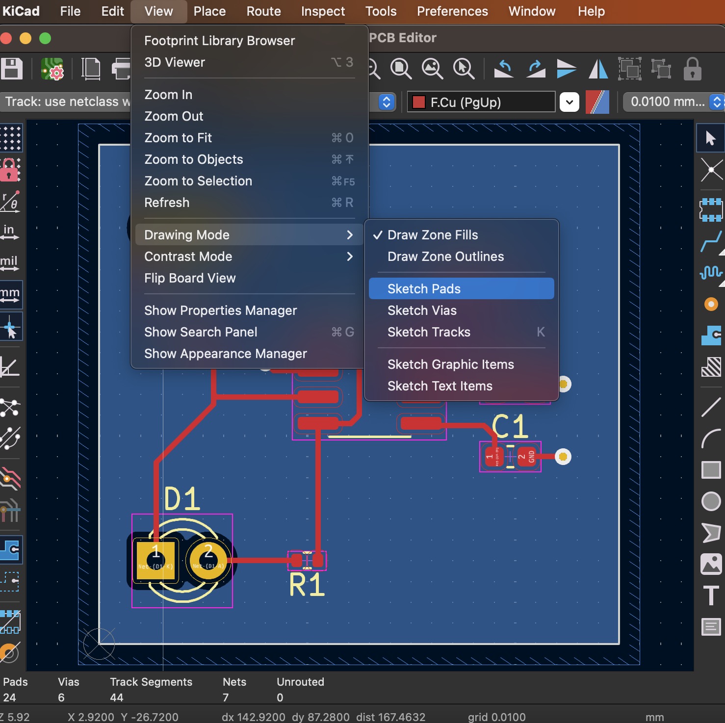
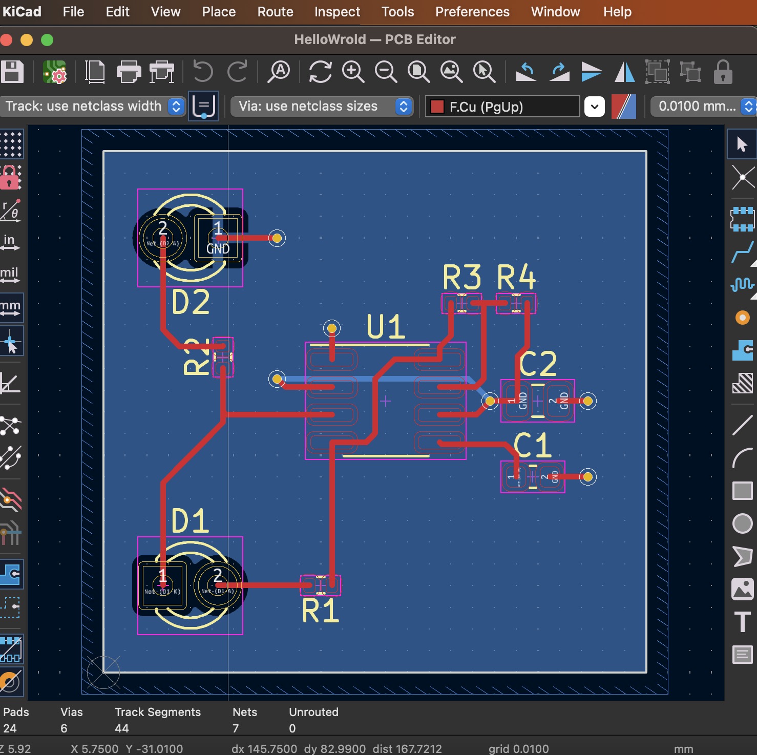
KiCad 8.x’s Sketch Pads & Vias
View ▷ Drawing Mode ▷ Sketch Pads & Sketch Vias
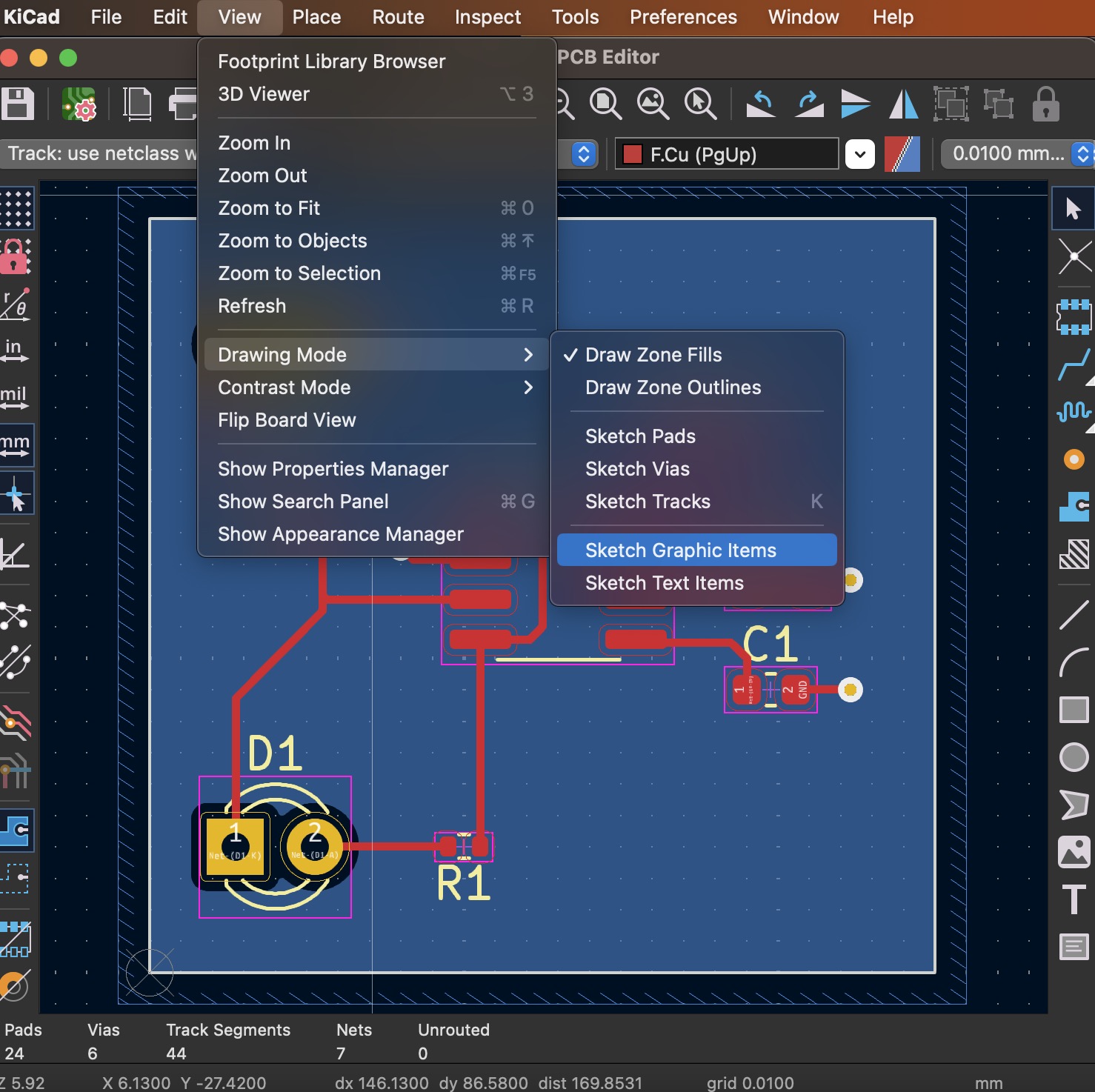
KiCad 8.x’s Sketch Graphic & Text
View ▷ Drawing Mode ▷ Sketch Graphic Items & Sketch Text Items
Conclusion
These tips can help you take advantage of transparency in KiCad 8.x to improve PCB design readability and speed up routing.
